DS1921G Просмотр технического описания (PDF) - Maxim Integrated
Номер в каталоге
Компоненты Описание
производитель
DS1921G Datasheet PDF : 42 Pages
| |||
MSB
8-BIT
CRC CODE
MSB
LSB MSB
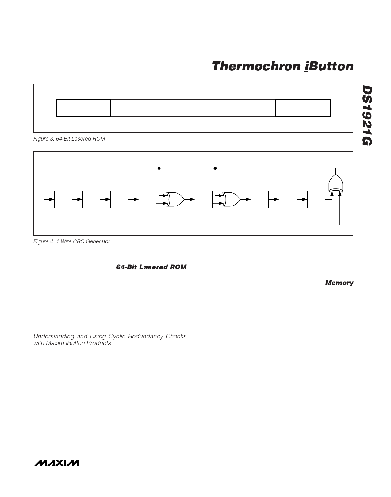
Figure 3. 64-Bit Lasered ROM
Thermochron iButton
48-BIT SERIAL NUMBER
LSB
8-BIT FAMILY CODE
(21h)
LSB MSB
LSB
POLYNOMIAL = X8 + X5 + X4 + 1
1ST
STAGE
2ND
STAGE
3RD
STAGE
4TH
STAGE
X0
X1
X2
X3
Figure 4. 1-Wire CRC Generator
5TH
STAGE
X4
6TH
STAGE
7TH
STAGE
8TH
STAGE
X5
X6
X7
X8
INPUT DATA
64-Bit Lasered ROM
Each DS1921G contains a unique ROM code that is 64
bits long. The first 8 bits are a 1-Wire family code. The
next 48 bits are a unique serial number. The last 8 bits
are a cyclic redundancy check (CRC) of the first 56 bits
(see Figure 3 for details). The 1-Wire CRC is generated
using a polynomial generator consisting of a shift regis-
ter and XOR gates as shown in Figure 4. The polynomi-
al is X8 + X5 + X4 + 1. Additional information about the
1-Wire CRC is available in Application Note 27:
Understanding and Using Cyclic Redundancy Checks
with Maxim iButton Products.
The Shift register bits are initialized to 0. Then, starting
with the least significant bit of the family code, one bit
at a time is shifted in. After the 8th bit of the family code
has been entered, the serial number is then entered.
After the 48th bit of the serial number has been
entered, the Shift register contains the CRC value.
Shifting in the 8 bits of CRC returns the Shift register to
all zeros.
Memory
Figure 5 shows the DS1921G memory map. The 4096-bit
general-purpose SRAM makes up pages 0 to 15. The
timekeeping, control, and counter registers fill page 16,
called register page (see Figure 6). Pages 17, 18, and
19 are assigned to storing the alarm timestamps and
durations. The temperature histogram bins begin at page
64 and use up to four pages. The data-log memory cov-
ers pages 128 to 191. Memory pages 20 to 63, 68 to
127, and 192 to 255 are reserved for future extensions.
The scratchpad is an additional page that acts as a
buffer when writing to the SRAM or the register page.
The memory pages 17 and higher are read only for the
user. They are written to or erased solely under the
supervision of the on-chip control logic.
_______________________________________________________________________________________ 9
Share Link: 