DS1624(2015) Просмотр технического описания (PDF) - Maxim Integrated
Номер в каталоге
Компоненты Описание
производитель
DS1624 Datasheet PDF : 14 Pages
| |||
DS1624
Pin Configurations
TOP VIEW
SDA 1
SCL 2
N.C. 3
GND 4
+
DS1624
8 VDD
7 A0
6 A1
5 A2
SO (208 mils)
1 SDA
VDD 8
DS1624
2 SCL
A0 7
3 N.C.
A1 6
4 GND
A2 5
PDIP (300 mils)
Digital Thermometer and Memory
Pin Description
PIN NAME
FUNCTION
1
SDA
Data Input/Output Pin for 2-Wire Serial
Communication Port
2
SCL
Clock Input/Output Pin for 2-Wire Serial
Communication Port
3
N.C. No Connection. No Internal Connection.
4
GND Ground
5
A2
Address Input
6
A1
Address Input
7
A0
Address Input
8
VDD 2.7V to 5.5V Input Power-Supply Voltage
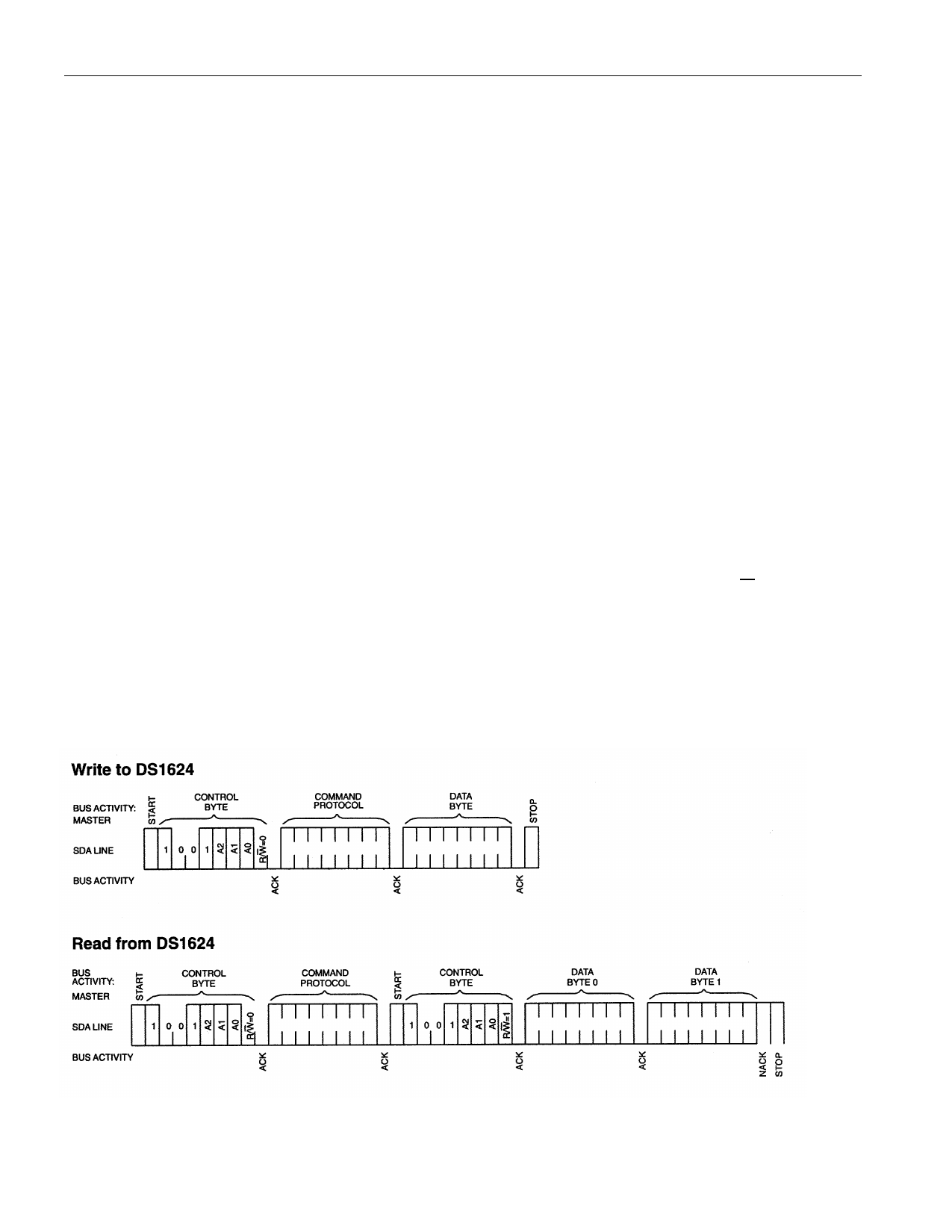
Detailed Description
2-Wire Serial Data Bus
The DS1624 supports a bidirectional two-wire bus and
data transmission protocol. A device that sends data onto
the bus is defined as a transmitter, and a device receiving
data as a receiver. The device that controls the message
is called a “master.” The devices that are controlled by
the master are “slaves.” The bus must be controlled by
a master device which generates the serial clock (SCL),
controls the bus access, and generates the START and
STOP conditions. The DS1624 operates as a slave on
the two-wire bus. Connections to the bus are made via
the open-drain I/O lines SDA and SCL. The following bus
protocol has been defined (see Figure 2):
●● Data transfer can be initiated only when the bus is
not busy.
●● During data transfer, the data line must remain stable
whenever the clock line is high. Changes in the data
line while the clock line is high are interpreted as
control signals.
Accordingly, the following bus conditions have been
defined:
Bus Not Busy: Both data and clock lines remain high.
Start Data Transfer: A change in the state of the data
line, from high to low, while the clock is high, defines a
START condition.
Stop Data Transfer: A change in the state of the data
line, from low to high, while the clock line is high, defines
the STOP condition.
Data Valid: The state of the data line represents valid
data when, after a START condition, the data line is stable
for the duration of the high period of the clock signal. The
data on the line must be changed during the low period of
the clock signal. There is one clock pulse per bit of data.
Each data transfer is initiated with a START condition and
terminated with a STOP condition. The number of data
bytes transferred between START and STOP conditions
is not limited, and is determined by the master device.
www.maximintegrated.com
Maxim Integrated │ 5
Share Link: 