DS1624(2015) Просмотр технического описания (PDF) - Maxim Integrated
Номер в каталоге
Компоненты Описание
производитель
DS1624 Datasheet PDF : 14 Pages
| |||
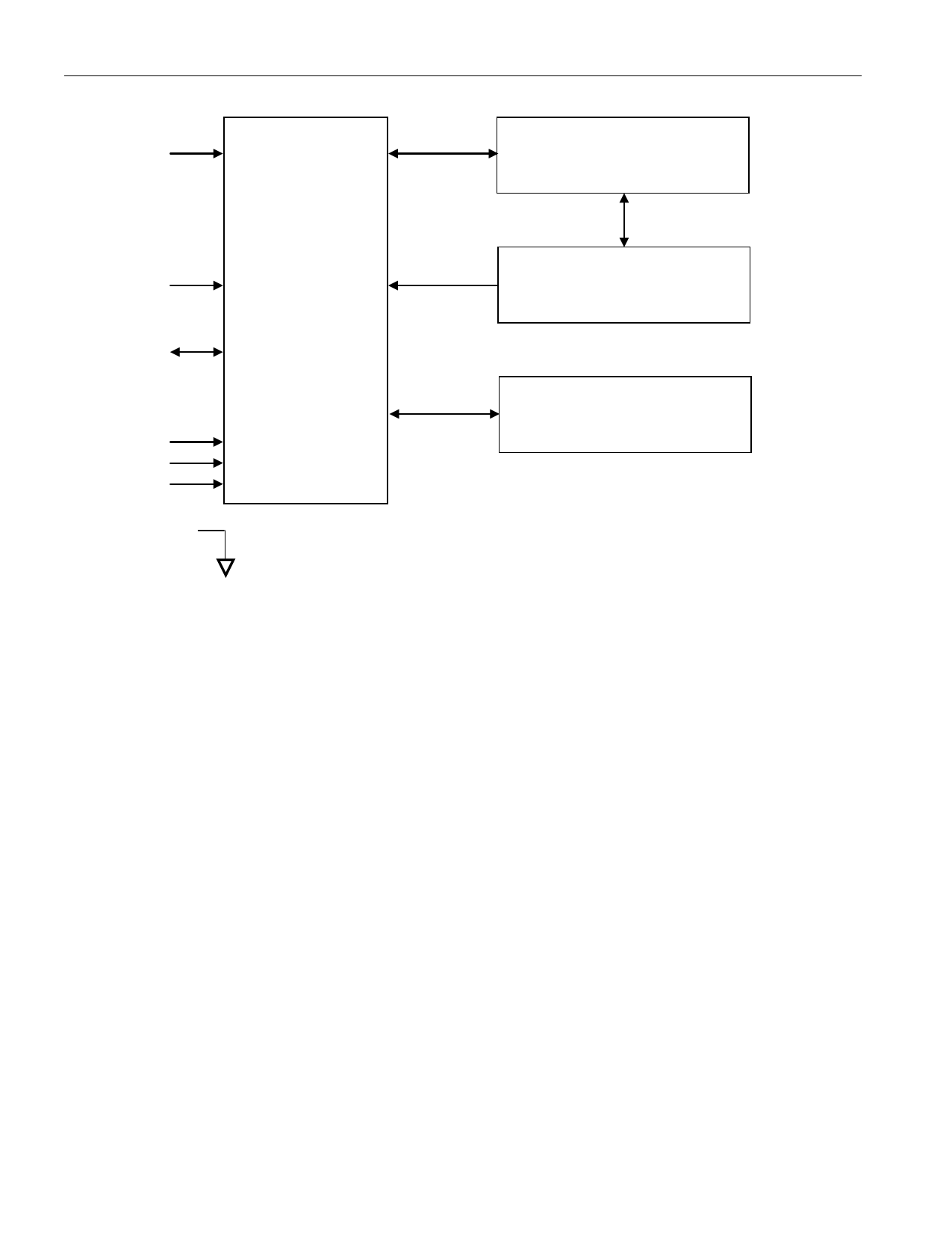
DS1624
Digital Thermometer and Memory
AC Electrical Characteristics
(VDD = 2.7V to 5.5V, TA = -55°C to +125°C, unless otherwise noted. All values referred to VIH = 0.9VDD and VIL = 0.1VDD.)
PARAMETER
SYMBOL
CONDITIONS
MIN TYP MAX UNITS
Temperature Conversion Time
EEPROM Write Cycle Time
EEPROM Endurance
EEPROM Data Retention
SLK Clock Frequency
tTC
tWR
NEEWR
tEEDR
fSCL
0°C to +70°C (Note 8)
-20°C to +70°C
TA = +25°C
-40°C to +70°C
(Note 9)
Fast mode
Standard mode
(Note 10)
200
ms
50
ms
10k
20k
40k
80k
Write
Cycles
10
20
Years
0
400
kHz
0
100
Bus Free Time Between a STOP
and START Condition
tBUF
Fast mode
Standard mode
(Note 10)
1.3
4.7
µs
Hold Time (Repeated)
START Condition
Fast mode
0.6
tHD:STA
Standard mode
(Notes 10, 11)
4.0
µs
Fast mode
1.3
Low Period of SCL Clock
tLOW
Standard mode
(Note 10)
4.7
µs
Fast mode
0.6
High Period of SCL Clock
tHIGH
Standard mode
(Note 10)
4.0
µs
Setup Time for a Repeated START
Condition
tSU:STA
Fast mode
Standard mode
(Note 10)
0.6
4.7
µs
Data Hold Time
Fast mode
0
tHD:DAT
Standard mode
(Note 10)
0
0.9
µs
0.9
Data Setup Time
tSU:DAT
Fast mode
Standard mode
(Notes 10, 11,
12)
100
250
ns
Rise Time of Both SDA and SCL
Signals
Fall Time of Both SDA and SCL
Signals
Setup Time for STOP Condition
tR
tF
tSU:STO
Fast mode
Standard mode
Fast mode
Standard mode
Fast mode
Standard mode
(Notes 8, 10, 12)
(Notes 8, 10, 12)
(Note 10)
20 + 0.1CB
20 + 0.1CB
20 + 0.1CB
20 + 0.1CB
0.6
4.0
300
ns
1000
300
ns
300
µs
Capacitive Load for Each Bus Line
CB
Input Capacitance
CI
400
pF
5
pF
Note 2: All voltages are referenced to ground.
Note 3: Limits are 100% production tested at TA = +25°C and/or TA = +85°C. Limits over the operating temperature range and
relevant supply voltage are guaranteed by design and characterization.
Note 4:
Note 5:
Note 6:
Note 7:
I/O pins of fast mode devices must not obstruct the SDA and SCL lines if VDD is switched off.
ICC specified with SDA pin open.
ICC specified with VCC at 5.0V and SDA, SCL = 5.0V, 0°C to +70°C.
EEPROM inactive, temperature sensor in shutdown mode.
Note 8: For example, if CB = 300pF, then tR(MIN) = tF(MIN) = 50ns.
Note 9: Write occurs between 0°C and +70°C.
Note 10: See the timing diagram (Figure 2). All timing is referenced to 0.9VDD and 0.1VDD.
Note 11: After this period, the first clock pulse is generated.
Note 12: A fast mode device can be used in a standard mode system, but the requirement tSU:DAT ≥ 250ns must then be met. This
is automatically the case if the device does not stretch the low period of the SCL signal. If such a device does stretch the
low period of the SCL signal, it must output the next data bit to the SDA line tR(MAX) + tSU:DAT = 1000 + 250 = 1250ns
before the SCL line is released.
www.maximintegrated.com
Maxim Integrated │ 3
Share Link: 