D8254 Просмотр технического описания (PDF) - Digital Core Design
Номер в каталоге
Компоненты Описание
производитель
D8254 Datasheet PDF : 4 Pages
| |||
been selected by holding CS low. The WR
and CLK signals should be synchronous. This
is accomplished by using a CLK input signal
to the D8254 counters which is a derivative of
the system clock source. Another technique
is to externally synchronize the WR and CLK
input signals. This is done by gating WR with
CLK.
Data Bus Buffer 8-bit buffer is used to inter-
face the D8254 to the system bus.
Control Word - The Control Word Register is
selected by the Read/Write Logic when
ADDR(1:0) = 11. If the CPU then does a write
operation to the D8254, the data is stored in
the Control Word Register and is interpreted
as a Control Word used to define the opera-
tion of the Counters.
COUNTERS BLOCK
DIAGRAM
All three Counters (0, 1, 2) are functionally
identical and fully independent. Each can
work as a 16 bit wide Binary or BCD counter,
in one of the six available modes:
● Interrupt on terminal count
● Hardware retriggerable One-Shot
● Rate Generator
● Square wave mode
● Software triggered strobe
● Hardware triggered strobe
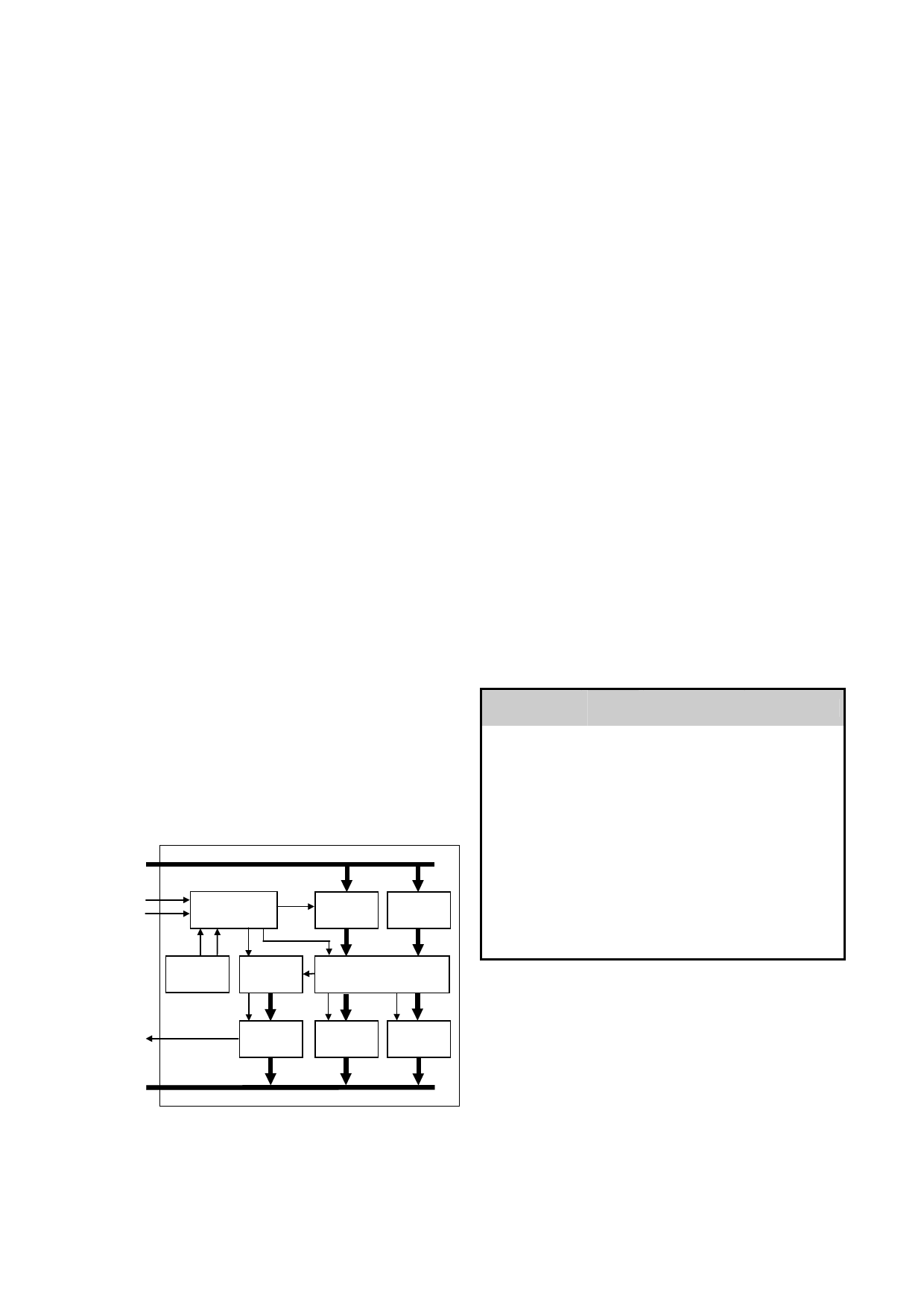
The internal block diagram of a single counter
is shown in Figure below.
datai(7:0)
clkn
gaten
Control
Unit
CRM
CRL
Ctrl. Word
Satus
Register
Register
CE
settable synchronous down BIN/BCD
counter.
Status Register, Status Latch – Status
register contains actual mode declaration and
value of output signal. Latched in Status
Latch, after receiving Read-Back Command
with STATUS Bit = 0.
Control Unit – Controls read/write operation
and decrementing of CE.
CR M, CR L – Input data registers. When
new count is written to counter, the count is
written in the CR and later transferred to CE.
OL L, OL M – Output data registers. Latched
when the suitable Counter Latch Command is
sent to the D8254.
Control Word - The Control Word Register is
selected by the Read/Write Logic when
ADDR(1:0) = 11. If the CPU then does a write
operation to the D8254, the data is stored in
the Control Word Register and is interpreted
as a Control Word used to define the opera-
tion of the Counters.
PERFORMANCE
The following table gives a survey about
the Core area and performance in the AL-
TERA® devices after Place & Route:
Device
Speed
grade
Logic Cells
Fmax
CYCLONE
-6
150 MHz
CYCLONE 2 -6
166 MHz
STRATIX
-5
181 MHz
STRATIX 2
-3
238 MHz
STRATIXGX -5
185 MHz
MERCURY
-5
135 MHz
EXCALIBUR -1
108 MHz
APEX II
-7
140 MHz
APEX20KC -7
129 MHz
APEX20KE
-1
105 MHz
APEX20K
-1V
88 MHz
ACEX1K
-1
99 MHz
FLEX10KE
-1
102 MHz
Core performance in ALTERA® devices
outn
Status
Latch
OLM
OLL
datao(7:0)
The central element of each Counter is CE
module - Counting Element – 16 bit pre-
All trademarks mentioned in this document
are trademarks of their respective owners.
http://www.DigitalCoreDesign.com
http://www.dcd.pl
Copyright 1999-2007 DCD – Digital Core Design. All Rights Reserved.
Share Link: 