CY7C9235-270JC Просмотр технического описания (PDF) - Cypress Semiconductor
Номер в каталоге
Компоненты Описание
производитель
CY7C9235-270JC Datasheet PDF : 8 Pages
| |||
PRELIMINARY
CY7C9235
using the ENA and ENN inputs, or by placing a C5.0 character
on the PD9–0 inputs when one of the two enables is active.
If the generation of K28.5 fill characters is to be controlled
using the ENA or ENN inputs, the SC/D_EN input should be
driven LOW or connected to VSS. This will insure that the PD0
data bit is not routed to the output register by forcing the Q0
output to always be LOW.
If the generation of a K28.5 characters is controlled by trans-
mission of a C5.0 character, the SC/D_EN input must be HIGH
to allow the PD0 input to be propagated to the Q0 output.
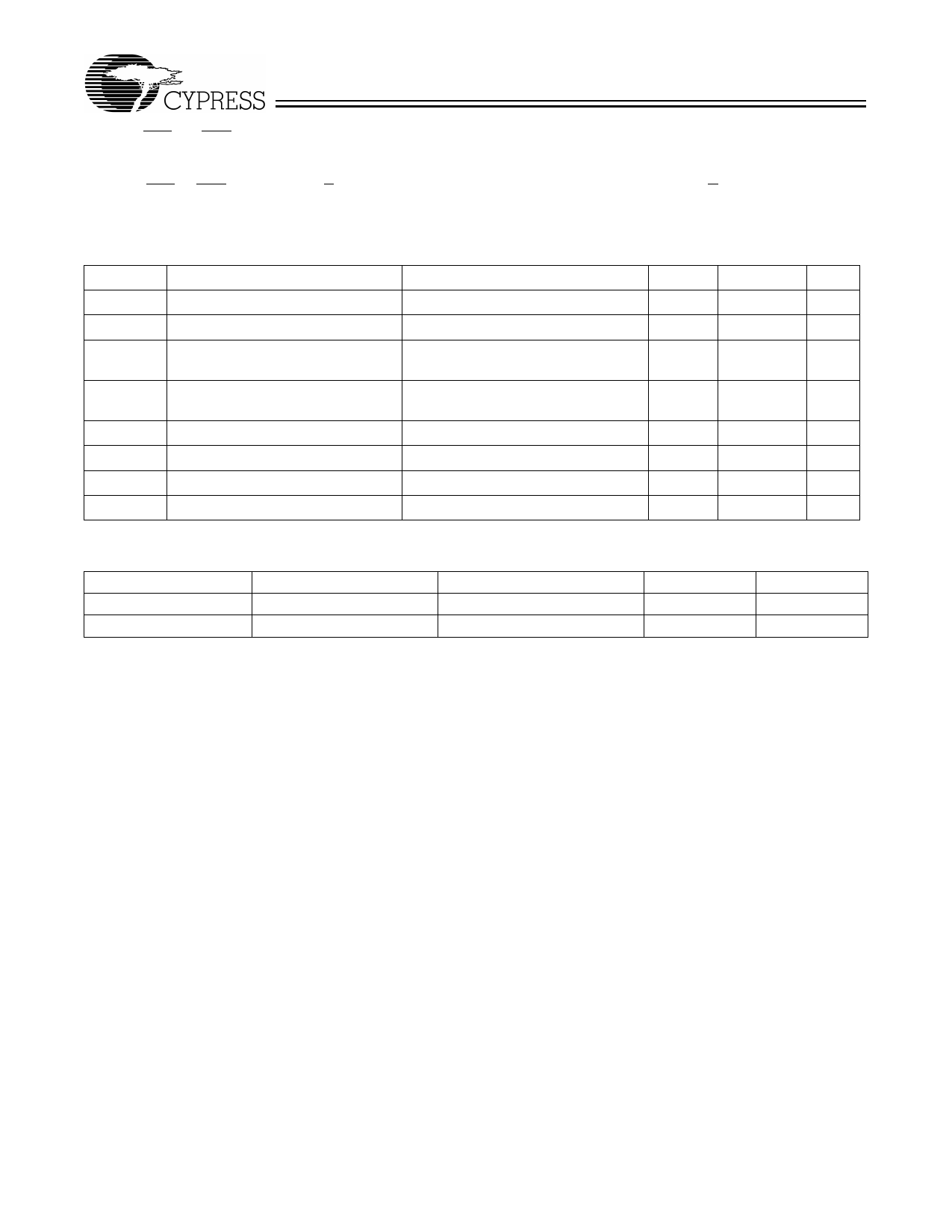
Electrical Characteristics Over the Operating Range
Parameter
Description
VOH
Output HIGH Voltage
VOL
Output LOW Voltage
VIH
Input HIGH Voltage
VIL
Input LOW Voltage
IIX
Input Load Current
IOZ
Output Leakage Current
IOS
Output Short Circuit Current[3,4]
ICC
Power Supply Current
Test Conditions
VCC=Min., IOH = −3.2 mA
VCC=Min., IOL = 16.0 mA
Guaranteed Input Logical HIGH
Voltage for all Inputs[2]
Guaranteed Input Logical HIGH
Voltage for all Inputs[2]
VI = VCC or VSS
VO = VCC or VSS
VCC = Max., VOUT = 0.5V
VIN, VI/O = VCC or VSS
Min.
2.4
2.0
–0.5
−10
−50
−10
Max.
Unit
V
0.5
V
7.0
V
0.8
V
+10
µA
+50
µA
− 80
mA
mA
Capacitance[4]
Parameter
Description
Test Conditions
Max.
Unit
CIN
Input Capacitance
VIN = 5.0V at f = 1 MHz
10
pF
COUT
Output Capacitance
VOUT = 5.0V at f = 1 MHz
12
pF
Notes:
1. Single Power Supply: The voltage on any input or I/O pin cannot exceed the power pin during power-up.
2. These are absolute values with respect to device ground. All overshoots due to system or tester noise are included.
3. Not more than one output should be tested at a time. Duration of the short circuit should not exceed 1 second. VOUT = 0.5V has been chosen to avoid test
problems caused by tester ground degradation.
4. Tested initially and after any design or process changes that may affect these parameters.
Document #: 38-02012 Rev. *A
Page 5 of 8
Share Link: 