CY7C63001C Просмотр технического описания (PDF) - Cypress Semiconductor
Номер в каталоге
Компоненты Описание
производитель
CY7C63001C Datasheet PDF : 28 Pages
| |||
CY7C63001C
CY7C63101C
b7
Reserved
0
b6
WDR
R/W
0
b5
USBR
b4
POR
b3
SUSPEND
b2
Reserved
b1
Reserved
R/W
R/W
R/W
0
1
0
0
0
Figure 6-3. Status and Control Register (SCR - Address 0xFF)
b0
RUN
R/W
1
6.3.1 Power-On Reset (POR)
Power-On Reset (POR) occurs every time the power to the
device is switched on. Bit 4 of the Status and Control Register
is set to record this event (the register contents are set to
00011001 by the POR). The USB Controller is placed in
suspended mode at the end of POR to conserve power (the
clock oscillator, the timers, and the interrupt logic are turned
off in suspend mode). After POR, only a non-idle USB Bus
state terminates the suspend mode. The microcontroller then
begins execution from ROM address 0x00.
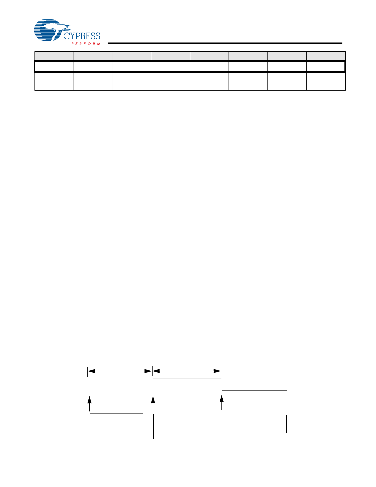
6.3.2 Watch Dog Reset (WDR)
The Watch Dog Timer Reset (WDR) occurs when the Most
Significant Bit of the 4-bit Watch Dog Timer Register transi-
tions from LOW to HIGH. Writing any value to the write-only
Watch Dog Restart Register at 0x21 clears the timer (firmware
should periodically write to the Watch Dog Restart Register in
the ‘main loop’ of firmware). The Watch Dog timer is clocked
by a 1.024-ms clock from the free-running timer. If 8 clocks
occur between writes to the timer, a WDR occurs and bit 6 of
the Status and Control Register is set to record the event. A
Watch Dog Timer Reset lasts for 8.192 ms, at which time the
microcontroller begins execution at ROM address 0x00. The
USB transmitter is disabled by a Watch Dog Reset because
the USB Device Address Register is cleared (otherwise, the
USB Controller would respond to all address 0 transactions).
The transmitter remains disabled until the WDR bit (bit 6) in
the Status and Control Register is reset to 0 by firmware.
6.3.3 USB Bus Reset
The USB Controller recognizes a USB Reset when a Single
Ended Zero (SE0) condition persists for at least 8–16 µs (the
Reset may be recognized for an SE0 as short as 8 µs, but it is
always recognized for an SE0 longer than 16 µs). SE0 is the
condition in which both the D+ line and the D– line are LOW.
Bit 5 of the Status and Control Register is set to record this
event. If the USB reset happens while the device is
suspended, the suspend condition is cleared and the clock
oscillator is restarted. However, the microcontroller is not
released until the USB reset is removed.
6.4 Instant-on Feature (Suspend Mode)
The USB Controller can be placed in a low-power state by
setting the Suspend bit (bit 3) of the Status and Control
register. All logic blocks in the device are turned off except the
USB receiver, the GPIO interrupt logic, and the Cext interrupt
logic. The clock oscillator and the free-running and watch dog
timers are shut down.
The suspend mode is terminated when one of the following
three conditions occur:
1. USB activity
2. A GPIO interrupt
3. Cext interrupt
The clock oscillator, GPIO, and timers restart immediately
upon exiting suspend mode. The USB engine and microcon-
troller return to a fully functional state no more than 256 µs
later. Before servicing any interrupt requests, the microcon-
troller executes the instruction following the I/O write that
placed the device into suspend mode.
Both the GPIO interrupt and the Cext interrupt allow the USB
Controller to wake-up periodically and poll potentiometers,
optics, and other system components while maintaining a very
low average power consumption. The Cext Interrupt is
preferred for lowest power consumption.
For Cext to generate an “Instant-on” interrupt, the pin must be
connected to ground with an external capacitor and connected
to VCC with an external resistor. A “0” is written to the Cext
register located at I/O address 0x22 to discharge the capacitor.
Then, a “1” is written to disable the open-drain output driver. A
Schmitt trigger input circuit monitors the input and generates
a wake-up interrupt when the input voltage rises above the
input threshold. By changing the values of the external resistor
and capacitor, the user can fine tune the charge rate of the R-C
timing circuit. The format of the Cext register is shown in
7.168 to
8.192 ms
8.192 ms
Last write to
Watchdog Timer
Register
No write to WDT
register, so WDR
goes HIGH
Execution begins at
Reset Vector 0x00
Figure 1. Watch Dog Reset (WDR)
Document #: 38-08026 Rev. *B
Page 7 of 28
Share Link: 