CY7C1359A-100AC Просмотр технического описания (PDF) - Cypress Semiconductor
Номер в каталоге
Компоненты Описание
производитель
CY7C1359A-100AC Datasheet PDF : 24 Pages
| |||
CY7C1359A/GVT71256T18
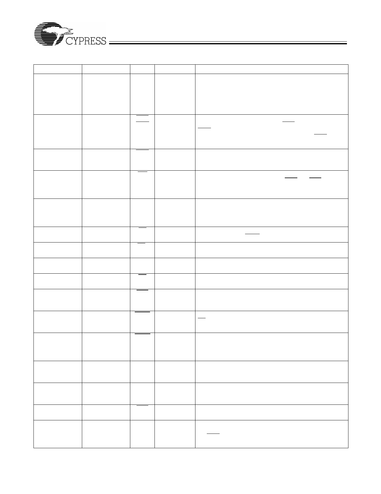
Pin Descriptions
BGA Pins
4P
4N
2A, 3A, 5A, 6A,
3B, 5B, 2C, 3C,
5C, 6C, 2R, 6R,
2T, 3T, 5T, 6T
5L
3G
4M
4H
4K
4E
6B
2B
4F
4G
4A
4B
3R
7T
7N
6M
TQFP Pins
37
36
35, 34, 33, 32,
100, 99, 82, 81,
80, 48, 47, 46, 45,
44, 49, 50
93
94
87
88
89
98
92
97
86
83
84
85
31
64
52
53
Name
A0
A1
A
Type
Input-
Synchronous
Description
Addresses: These inputs are registered and must meet the
set-up and hold times around the rising edge of CLK. The
burst counter generates internal addresses associated with
A0 and A1, during burst cycle and wait cycle.
WEL
WEH
Input-
Synchronous
Byte Write Enables: A byte write enable is LOW for a WRITE
cycle and HIGH for a READ cycle. WEL controls DQ1–DQ9.
WEH controls DQ10–DQ18. Data I/O are high impedance if
either of these inputs are LOW, conditioned by BWE being
LOW.
BWE
Input-
Write Enable: This active LOW input gates byte write opera-
Synchronous tions and must meet the set-up and hold times around the
rising edge of CLK.
GW
Input-
Global Write: This active LOW input allows a full 18-bit
Synchronous WRITE to occur independent of the BWE and WEn lines and
must meet the set-up and hold times around the rising edge
of CLK.
CLK
Input-
Clock: This signal registers the addresses, data, chip en-
Synchronous ables, write control, and data input enable control input on its
rising edge. All synchronous inputs must meet set-up and
hold times around the clock’s rising edge.
CE
Input-
Chip Enable: This active LOW input is used to enable the
Synchronous device and to gate ADSP.
CE2
Input-
Chip Enable: This active LOW input is used to enable the
Synchronous device.
CE2
input-
Chip Enable: This active HIGH input is used to enable the
Synchronous device.
OE
Input
Output Enable: This active LOW asynchronous input enables
the data output drivers.
ADV
Input-
Address Advance: This active LOW input is used to control
Synchronous the internal burst counter. A HIGH on this pin generates wait
cycle (no address advance).
ADSP
Input-
Address Status Processor: This active LOW input, along with
Synchronous CE being LOW, causes a new external address to be regis-
tered and a READ cycle is initiated using the new address.
ADSC
Input-
Synchronous
Address Status Controller: This active LOW input causes de-
vice to be deselected or selected along with new external
address to be registered. A READ or WRITE cycle is initiated
depending upon write control inputs.
MODE
Input-
Static
Mode: This input selects the burst sequence. A LOW on this
pin selects Linear Burst. A NC or HIGH on this pin selects
Interleaved Burst.
ZZ
Input-
Snooze: This active HIGH input puts the device in low power
Asynchronous consumption standby mode. For normal operation, this input
has to be either LOW or NC (No Connect).
DEN
Input-
Data Input Enable: This active LOW input is used to control
Synchronous the update of data input registers.
MATCH
Output
Match Output: MATCH will be HIGH if data in the data input
registers match the data stored in the memory array, assum-
ing MOE being LOW. MATCH will be LOW if data do not
match.
Document #: 38-05120 Rev. **
Page 4 of 24
Share Link: 