CY7C1340A-66 Просмотр технического описания (PDF) - Cypress Semiconductor
Номер в каталоге
Компоненты Описание
производитель
CY7C1340A-66 Datasheet PDF : 12 Pages
| |||
CY7C1340A
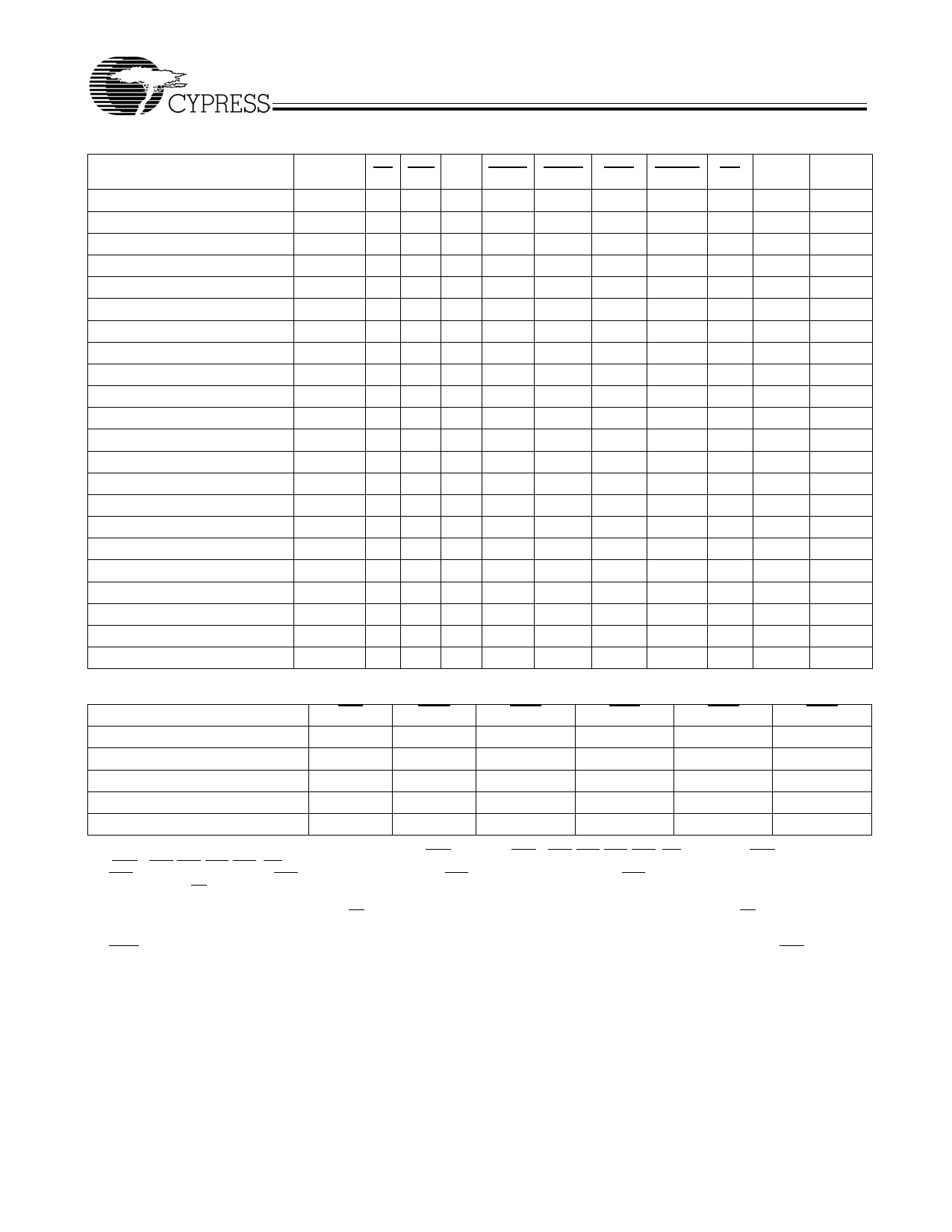
Truth Table[2, 3, 4, 5, 6, 7, 8]
Operation
Address
Used CE CE2 CE2 ADSP ADSC ADV WRITE OE
Deselected Cycle, Power-down None H X X
X
L
X
X
X
Deselected Cycle, Power-down None L X L
L
X
X
X
X
Deselected Cycle, Power-down None L H X
L
X
X
X
X
Deselected Cycle, Power-down None L X L
H
L
X
X
X
Deselected Cycle, Power-down None L H X
H
L
X
X
X
Read Cycle, Begin Burst
External L L H
L
X
X
X
L
Read Cycle, Begin Burst
External L L H
L
X
X
X
H
Write Cycle, Begin Burst
External L L H
H
L
X
L
X
Read Cycle, Begin Burst
External L L H
H
L
X
H
L
Read Cycle, Begin Burst
External L L H
H
L
X
H
H
Read Cycle, Continue Burst
Next X X X
H
H
L
H
L
Read Cycle, Continue Burst
Next X X X
H
H
L
H
H
Read Cycle, Continue Burst
Next H X X
X
H
L
H
L
Read Cycle, Continue Burst
Next H X X
X
H
L
H
H
Write Cycle, Continue Burst
Next X X X
H
H
L
L
X
Write Cycle, Continue Burst
Next H X X
X
H
L
L
X
Read Cycle, Suspend Burst
Current X X X
H
H
H
H
L
Read Cycle, Suspend Burst
Current X X X
H
H
H
H
H
Read Cycle, Suspend Burst
Current H X X
X
H
H
H
L
Read Cycle, Suspend Burst
Current H X X
X
H
H
H
H
Write Cycle, Suspend Burst
Current X X X
H
H
H
L
X
Write Cycle, Suspend Burst
Current H X X
X
H
H
L
X
CLK
L–H
L–H
L–H
L–H
L–H
L–H
L–H
L–H
L–H
L–H
L–H
L–H
L–H
L–H
L–H
L–H
L–H
L–H
L–H
L–H
L–H
L–H
DQ
High-Z
High-Z
High-Z
High-Z
High-Z
Q
High-Z
D
Q
High-Z
Q
High-Z
Q
High-Z
D
D
Q
High-Z
Q
High-Z
D
D
Partial Truth Table for Read/Write
FUNCTION
GW
BWE
BW1
BW2
BW3
BW4
Read
H
H
X
X
X
X
Read
H
L
H
H
H
H
Write one byte
H
L
L
H
H
H
Write all bytes
H
L
L
L
L
L
Write all bytes
L
X
X
X
X
X
Notes:
2. X means “Don’t Care.” H means logic HIGH. L means logic LOW. Write = L means [BWE + BW1*BW2*BW3*BW4]*GW equals LOW. Write = H means
[BWE + BW1*BW2*BW3*BW4]*GW equals HIGH.
3. BW1 enables Write to DQ1–DQ8. BW2 enables Write to DQ9–DQ16. BW3 enables Write to DQ17–DQ24. BW4 enables Write to DQ25–DQ32.
4. All inputs except OE must meet set-up and hold times around the rising edge (LOW–HIGH) of CLK.
5. Suspending burst generates Wait cycle.
6. For a Write operation following a Read operation, OE must be HIGH before the input data required set-up time plus High-Z time for OE and staying HIGH
throughout the input data hold time.
7. This device contains circuitry that will ensure the outputs will be in High-Z during power-up.
8. ADSP LOW along with chip being selected always initiates a Read cycle at the L–H edge of CLK. A Write cycle can be performed by setting Write LOW for the
CLK L–H edge of the subsequent wait cycle. Refer to Write timing diagram for clarification.
Document #: 38-05153 Rev. *C
Page 5 of 12
Share Link: 