CY7C1328F Просмотр технического описания (PDF) - Cypress Semiconductor
Номер в каталоге
Компоненты Описание
производитель
CY7C1328F Datasheet PDF : 17 Pages
| |||
CY7C1328F
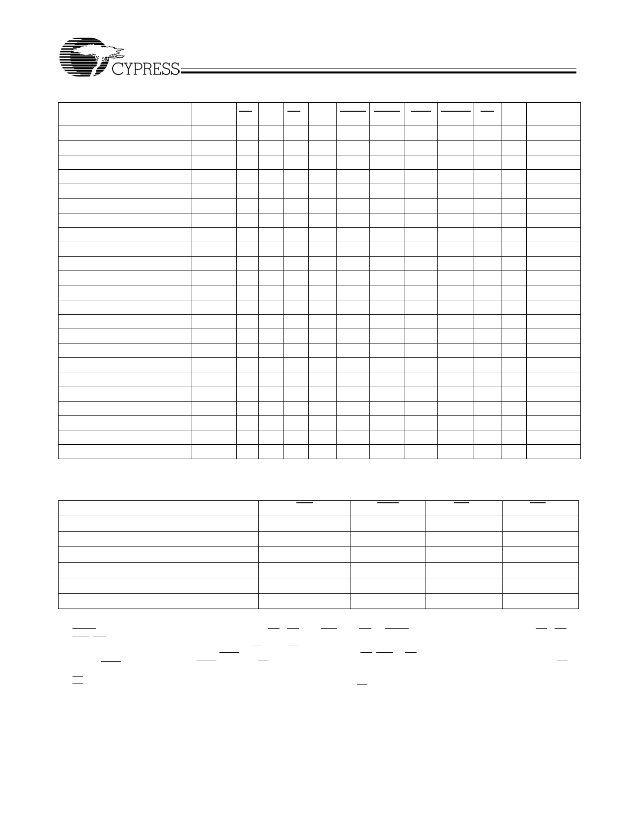
Truth Table [2, 3, 4, 5, 6]
Operation
Address
Used CE1 CE2 CE3 ZZ ADSP ADSC ADV WRITE OE CLK
DQ
Deselected Cycle, Power Down None H X X L
X
L
X
X
X L-H Three-State
Deselected Cycle, Power Down None L L X L
L
X
X
X
X L-H Three-State
Deselected Cycle, Power Down None L X H L
L
X
X
X
X L-H Three-State
Deselected Cycle, Power Down None L L X L
H
L
X
X
X L-H Three-State
Deselected Cycle, Power Down None L X H L
H
L
X
X
X L-H Three-State
ZZ Mode, Power-Down
None X X X H X
X
X
X
X X Three-State
Read Cycle, Begin Burst
External L H L L
L
X
X
X
L L-H
Q
Read Cycle, Begin Burst
External L H L L
L
X
X
X
H L-H Three-State
Write Cycle, Begin Burst
External L H L L
H
L
X
L
X L-H
D
Read Cycle, Begin Burst
External L H L L
H
L
X
H
L L-H
Q
Read Cycle, Begin Burst
External L H L L
H
L
X
H
H L-H Three-State
Read Cycle, Continue Burst
Next X X X L
H
H
L
H
L L-H
Q
Read Cycle, Continue Burst
Next X X X L
H
H
L
H
H L-H Three-State
Read Cycle, Continue Burst
Next H X X L
X
H
L
H
L L-H
Q
Read Cycle, Continue Burst
Next H X X L
X
H
L
H
H L-H Three-State
Write Cycle, Continue Burst
Next X X X L
H
H
L
L
X L-H
D
Write Cycle, Continue Burst
Next H X X L
X
H
L
L
X L-H
D
Read Cycle, Suspend Burst
Current X X X L
H
H
H
H
L L-H
Q
Read Cycle, Suspend Burst
Current X X X L
H
H
H
H
H L-H Three-State
Read Cycle, Suspend Burst
Current H X X L
X
H
H
H
L L-H
Q
Read Cycle, Suspend Burst
Current H X X L
X
H
H
H
H L-H Three-State
Write Cycle, Suspend Burst
Current X X X L
H
H
H
L
X L-H
D
Write Cycle, Suspend Burst
Current H X X L
X
H
H
L
X L-H
D
Truth Table for Read/Write[2]
Read
Function
GW
BWE
BWA
BWB
H
H
X
X
Read
H
L
H
H
Write byte A - (DQA and DQPA)
Write byte B - (DQB and DQPB)
Write all bytes
H
L
L
H
H
L
H
L
H
L
L
L
Write all bytes
L
X
X
X
Notes:
2. X = “Don't Care.” H = Logic HIGH, L = Logic LOW.
3. WRITE = L when any one or more Byte Write enable signals (BWA, BWB) and BWE = L or GW= L. WRITE = H when all Byte write enable signals (BWA, BWB),
BWE, GW = H.
4. The DQ pins are controlled by the current cycle and the OE signal. OE is asynchronous and is not sampled with the clock.
5. The SRAM always initiates a read cycle when ADSP is asserted, regardless of the state of GW, BWE, or BW[A:B]. Writes may occur only on subsequent clocks
after the ADSP or with the assertion of ADSC. As a result, OE must be driven HIGH prior to the start of the write cycle to allow the outputs to three-state. OE is
a don't care for the remainder of the write cycle.
6. OE is asynchronous and is not sampled with the clock rise. It is masked internally during write cycles. During a read cycle all data bits are Three-State when
OE is inactive or when the device is deselected, and all data bits behave as output when OE is active (LOW).
Document #: 38-05220 Rev. *A
Page 7 of 17
Share Link: 