OM7670 Просмотр технического описания (PDF) - Omnirel Corp => IRF
Номер в каталоге
Компоненты Описание
производитель
OM7670 Datasheet PDF : 3 Pages
| |||
OM7670 Series
OM7671 Series
3.3
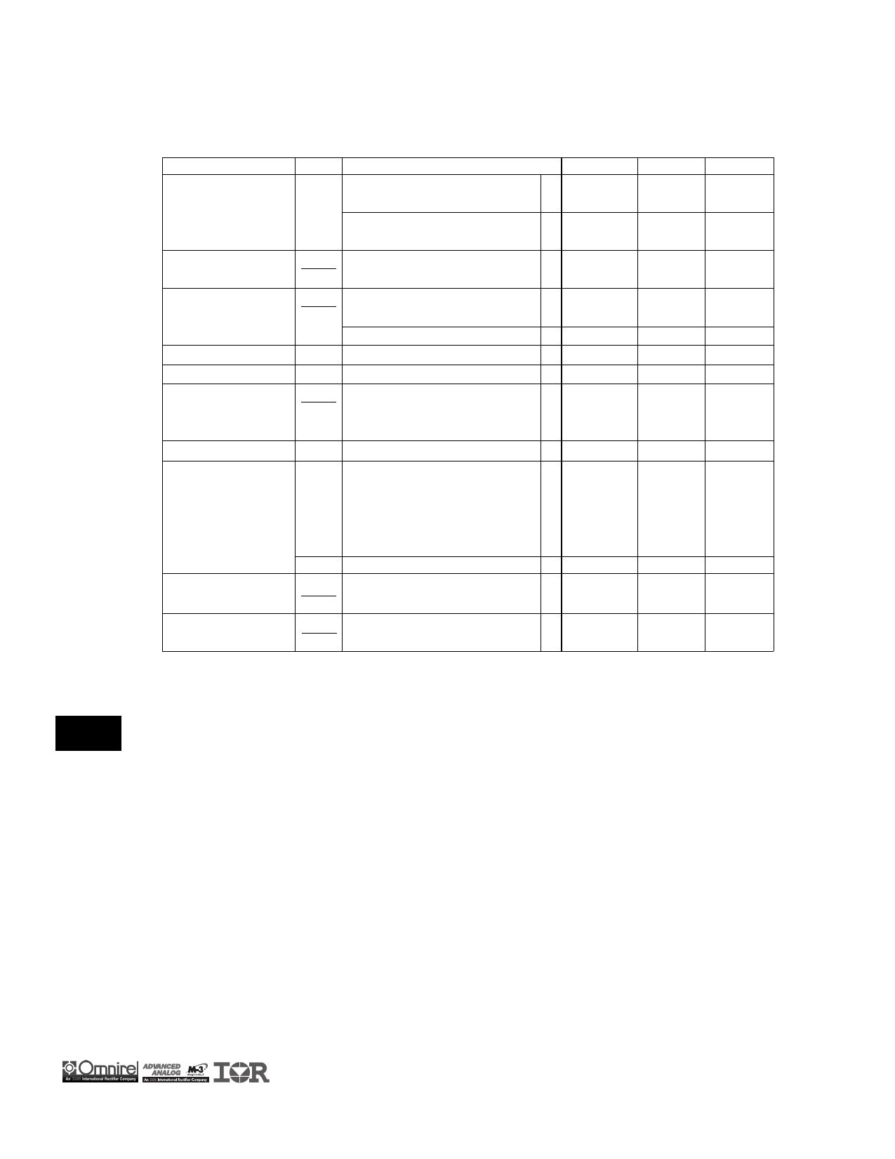
ELECTRICAL CHARACTERISTICS -55°C ≤ TA ≤ 125°C (unless otherwise specified)
Parameter
Symbol
Test Conditions
Min.
Max.
Output Voltage
Line Regulation
(Note 1)
Load Regulation
(Note 1)
Dropout Voltage
Thermal Regulation
Ripple Rejection
Quiescent Current
Current Limit
Temperature Stability
(Note 2)
VOUT
VIN = 5.0 V, IOUT = 10 mA
TA = 25° C
4.75 V ≤ VIN ≤ 18 V,
•
10 mA ≤ IOUT ≤ ILMIN
∆VOUT
4.5V ≤ VIN ≤ 18 V,
•
∆VIN
IOUT = 0 A
∆VOUT
VIN = 5.0 V, 0A ≤ IOUT ≤ ILMIN
∆IOUT
VDO
TA = 25° C
VIN = 5.0 V, 0A ≤ IOUT ≤ ILMIN
•
IOUT = ILMIN, ∆VREF = 1%
•
-
30 ms pulse, TA = +25° C
∆VIN
f = 120 Hz, CAdj = 25 µF,
•
∆VOUT
COUT = 25 µF (tantalum), IOUT = ILMIN,
VIN = 6.3 V
IQ
VIN = 18 V
•
IL
OM7670NK, VIN = 18 V
•
OM7670NM/ST/SM VIN = 18 V
•
OM7670N2, VIN = 18 V
•
OM7671NK, VIN = 18 V
•
OM7671NM/ST/SM, VIN = 18 V
•
VIN = 28 V, All Types
•
∆VOUT
-55° C ≤ TJ ≤ +125° C
∆T
3.267
3.325
60
1.5
1.3
.75
3.0
2.6
.050
3.333
3.365
12
15
25
1.5
0.04
10
3.5
2.5
1.50
5.0
4.5
--
1.55
Long Term Stability
∆VOUT
TA = +125° C, t = 1000 hrs
1.0
(Note 2)
∆T
Unit
V
V
mV
mV
mV
V
%/W
dB
mA
A
A
%
%
Notes:
1. Line and Load Regulation are measured at a constant junction temperature using a low duty cycle pulse technique.
Although power dissipation is internally limited, regulation is guaranteed up to the maximum power dissipation of 15W
for the OM7670 series and 30 watts for the OM7671 series (See Table 1). Power dissipation is determined by the
input/output differential voltage and the output current. Guaranteed maximum power dissipation will not be available over
the full input/output voltage range.
2. Guaranteed by design, characterization or correlation to other tested parameters.
3. The • denotes the specifications which apply over the full operating temperature range.
Share Link: 