CY14B101LA-SZ25XIT(2011) –ü—Ä–ĺ—Ā–ľ–ĺ—ā—Ä —ā–Ķ—Ö–Ĺ–ł—á–Ķ—Ā–ļ–ĺ–≥–ĺ –ĺ–Ņ–ł—Ā–į–Ĺ–ł—Ź (PDF) - Cypress Semiconductor
–Ě–ĺ–ľ–Ķ—Ä –≤ –ļ–į—ā–į–Ľ–ĺ–≥–Ķ
–ö–ĺ–ľ–Ņ–ĺ–Ĺ–Ķ–Ĺ—ā—č –ě–Ņ–ł—Ā–į–Ĺ–ł–Ķ
–Ņ—Ä–ĺ–ł–∑–≤–ĺ–ī–ł—ā–Ķ–Ľ—Ć
CY14B101LA-SZ25XIT Datasheet PDF : 26 Pages
| |||
CY14B101LA
CY14B101NA
1-Mbit (128 K √ó 8/64 K √ó 16) nvSRAM
1-Mbit (128 K x 8/64 K x 16) nvSRAM
Features
‚Ė† 20 ns, 25 ns, and 45 ns access times
‚Ė† Internally organized as 128 K √ó 8 (CY14B101LA) or 64 K √ó
16 (CY14B101NA)
‚Ė† Hands off automatic STORE on power-down with only a small
capacitor
‚Ė† STORE to QuantumTrap nonvolatile elements initiated by
software, device pin, or AutoStore on power-down
‚Ė† RECALL to SRAM initiated by software or power-up
‚Ė† Infinite read, write, and RECALL cycles
‚Ė† 1 million STORE cycles to QuantumTrap
‚Ė† 20 year data retention
‚Ė† Single 3 V +20% to -10% operation
‚Ė† Industrial temperature
‚Ė† Packages
‚Ěź 32-Pin small-outline integrated circuit (SOIC)
‚Ěź 44-/54-Pin thin small outline package (TSOP II)
‚Ěź 48-Pin shrink small-outline package (SSOP)
‚Ěź 48-Ball fine-pitch ball grid array (FBGA)
‚Ė† Pb-free and restriction of hazardous substances (RoHS)
compliant
Functional Description
The Cypress CY14B101LA/CY14B101NA is a fast static RAM
(SRAM), with a nonvolatile element in each memory cell. The
memory is organized as 128 K bytes of 8 bits each or 64 K words
of 16 bits each. The embedded nonvolatile elements incorporate
QuantumTrap technology, producing the world’s most reliable
nonvolatile memory. The SRAM provides infinite read and write
cycles, while independent nonvolatile data resides in the highly
reliable QuantumTrap cell. Data transfers from the SRAM to the
nonvolatile elements (the STORE operation) takes place
automatically at power-down. On power-up, data is restored to
the SRAM (the RECALL operation) from the nonvolatile memory.
Both the STORE and RECALL operations are also available
under software control.
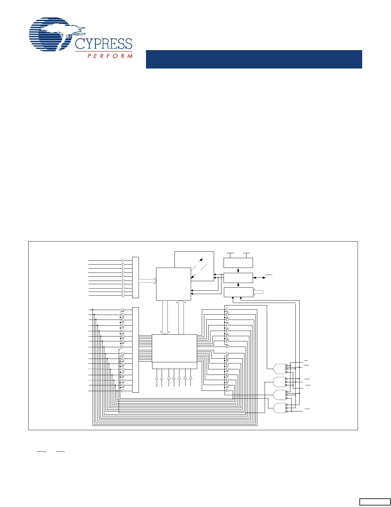
Logic Block Diagram[1, 2, 3]
4XDWUXP7UDS
9&&
9&$3
;
$
$
$
$
$
$
5
2
:
6725(
32:(5
&21752/
'
(
&
67$7,&5$0
5(&$//
6725(5(&$//
&21752/
+6%
$
2
$55$<
$
$
$
'
;
(
5
62)7:$5(
'(7(&7
$$
'4
'4
'4
'4
'4
'4
'4
'4
'4
'4
'4
'4
'4
'4
'4
'4
,
1
3
8
7
%
&2/801,2
8
)
)
(
5
&2/801'(&
6
$ $ $ $ $ $ $
2(
:(
&(
%/(
%+(
Notes
1. Address A0 - A16 for √ó8 configuration and Address A0 - A15 for √ó16 configuration.
2. Data DQ0 - DQ7 for √ó8 configuration and Data DQ0 - DQ15 for √ó16 configuration.
3. BHE and BLE are applicable for √ó16 configuration only.
Cypress Semiconductor Corporation ‚ÄĘ 198 Champion Court
Document #: 001-42879 Rev. *K
‚ÄĘ San Jose, CA 95134-1709 ‚ÄĘ 408-943-2600
Revised January 18, 2011
[+] Feedback
Share Link: 