CXK5V8512TM Просмотр технического описания (PDF) - Sony Semiconductor
Номер в каталоге
Компоненты Описание
производитель
CXK5V8512TM Datasheet PDF : 10 Pages
| |||
CXK5V8512TM
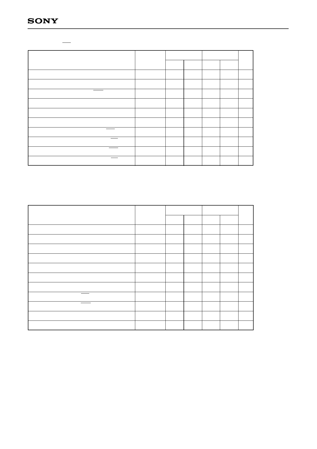
• Read cycle (WE = “H”)
(Vcc = 3.3V ± 0.3V, GND = 0V, Ta = –25 to +85°C)
Item
Read cycle time
Symbol
tRC
-85LLX
Min. Max.
85 —
-10LLX
Unit
Min. Max.
100 — ns
Address access time
tAA
— 85 — 100 ns
Chip enable access time (CE1)
tCO1
— 85 — 100 ns
Chip enable access time (CE2)
tCO2
— 85 — 100 ns
Output enable to output valid
tOE
— 40 — 50 ns
Output hold from address change
tOH
10 — 10 — ns
Chip enable to output in low Z (CE1, CE2) tLZ1, tLZ2
10 — 10 — ns
Output enable to output in low Z (OE)
tOLZ
5
—
5
— ns
Chip disable to output in high Z (CE1, CE2) tHZ1∗, tHZ2∗ —
35
—
40 ns
Output disable to output in high Z (OE)
tOHZ∗
— 30 — 35 ns
∗ tHZ1, tHZ2 and tOHZ are defined as the time required for outputs to turn to high impedance state and are not
referred to as output voltage levels.
• Write cycle
(Vcc = 3.3V ± 0.3V, GND = 0V, Ta = –25 to +85°C)
-85LLX
-10LLX
Item
Symbol
Unit
Min. Max. Min. Max.
Write cycle time
tWC
85 — 100 — ns
Address valid to end of write
tAW
70 — 80 — ns
Chip enable to end of write
tCW
70 — 80 — ns
Data to write time overlap
tDW
35 — 40 — ns
Data hold from write time
tDH
0
—
0
— ns
Write pulse width
tWP
60 — 70 — ns
Address setup time
tAS
0
—
0
— ns
Write recovery time (WE)
tWR
5
—
5
— ns
Write recovery time (CE1, CE2)
tWR1
5
—
5
— ns
Output active from end of write
Write to output in high Z
tOW
tWHZ∗
5
—
5
— ns
— 35 — 40 ns
∗ tWHZ is defined as the time required for outputs to turn to high impedance state and is not referred to as
output voltage level.
–5–
Share Link: 