CXK5V16100TM Просмотр технического описания (PDF) - Sony Semiconductor
Номер в каталоге
Компоненты Описание
производитель
CXK5V16100TM Datasheet PDF : 10 Pages
| |||
CXK5V16100TM
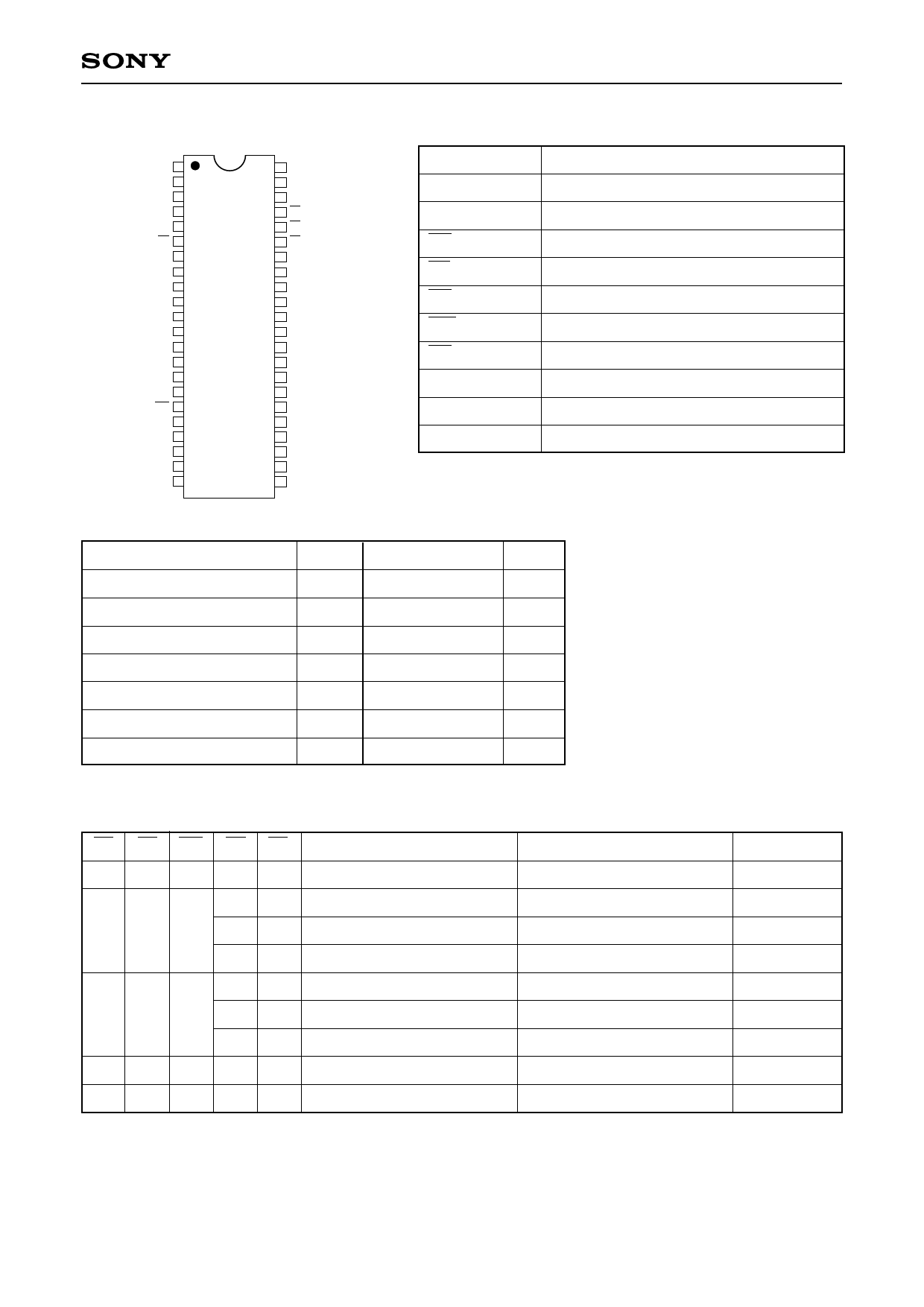
Pin Configuration (Top View)
A4 1
A3 2
A2 3
A1 4
A0 5
CE 6
I/O1 7
I/O2 8
I/O3 9
I/O4 10
Vcc 11
GND 12
I/O5 13
I/O6 14
I/O7 15
I/O8 16
WE 17
A15 18
A14 19
A13 20
A12 21
NC 22
44 A5
43 A6
42 A7
41 OE
40 UB
39 LB
38 I/O16
37 I/O15
36 I/O14
35 I/O13
34 GND
33 Vcc
32 I/O12
31 I/O11
30 I/O10
29 I/O9
28 NC
27 A8
26 A9
25 A10
24 A11
23 NC
Pin Description
Symbol
Description
A0 to A15
Address input
I/O1 to I/O16 Data input/output
CE
Chip enable input
LB
Byte enable input (I/O1 to I/O8)
UB
Byte enable input (I/O9 to I/O16)
WE
Write enable input
OE
Output enable input
VCC
+3.3V power supply
GND
Ground
NC
No connection
Absolute Maximum Ratings
(Ta = 25°C, GND = 0V)
Item
Symbol
Rating
Unit
Supply voltage
Input voltage
Input and output voltage
VCC
–0.5 to +4.6
V
VIN
–0.5∗ to VCC + 0.5 V
VI/O
–0.5∗ to VCC + 0.5 V
Allowable power dissipation PD
0.7
W
Operating temperature
Topr
–25 to +85
°C
Storage temperature
Tstg
–55 to +150
°C
Soldering temperature • time Tsolder
235 • 10
∗ VIN, VI/O = –3.0V Min. for pulse width less than 50ns.
°C • s
Truth Table
CE OE WE LB UB
I/O1 to I/O8
H × × × × Not selected
L L Read
L L H L H Read
H L High-Z
L L Write
L × L L H Write
H L Not Write/Hi-Z
L H H × × High-Z
L × × H H High-Z
I/O9 to I/O16
Not selected
Read
High-Z
Read
Write
Not Write/Hi-Z
Write
High-Z
High-Z
×: “H” or “L”
Vcc Current
ISB1, ISB2
ICC1, ICC2, ICC3
ICC1, ICC2, ICC3
ICC1, ICC2, ICC3
ICC1, ICC2, ICC3
ICC1, ICC2, ICC3
ICC1, ICC2, ICC3
ICC1, ICC2, ICC3
ICC1, ICC2, ICC3
–2–
Share Link: 