CXD4017R Просмотр технического описания (PDF) - Sony Semiconductor
Номер в каталоге
Компоненты Описание
производитель
CXD4017R
Sony Semiconductor

CXD4017R Datasheet PDF : 34 Pages
| |||
CXD4017R
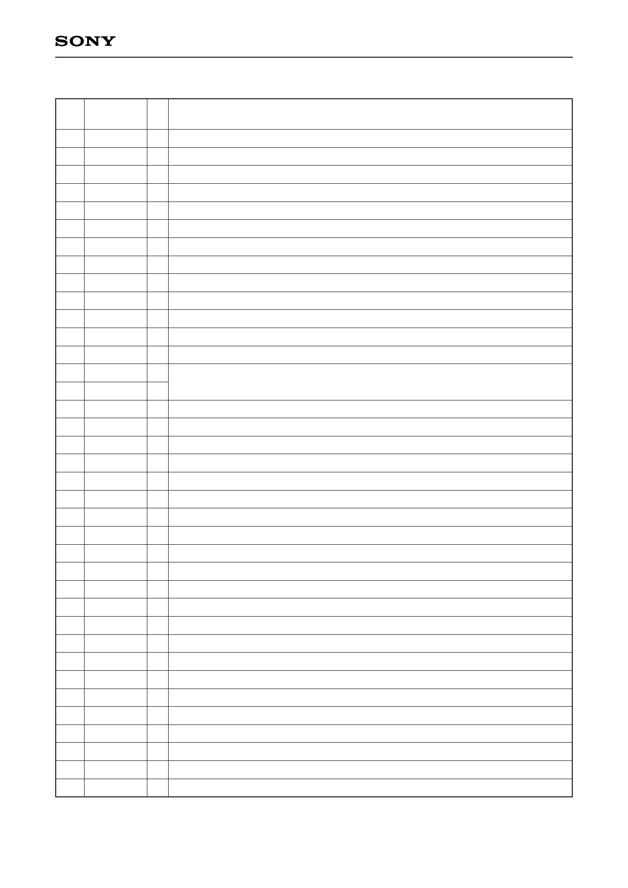
Pin Description
Pin
No.
Symbol I/O
Description
1 TEST12 I Test pin, normally fixed at low
2 TEST13 I Test pin, normally fixed at high
3 TEST14 I Test pin, normally fixed at high
4 VDDE
— Digital I/O power supply
5 VSS
— Digital GND
6 ADVRH
I RF ADC reference voltage input (high)
7 ADAVS — RF ADC analog GND
8 ADAVD — RF ADC analog power supply
9 ADVRL
I RF ADC reference voltage input (low)
10 ADVIN
I RF ADC input
11 VDDE
— Digital I/O power supply
12 VSS
— Digital GND
13 XRST
I Reset (negative logic)
14 DIFM0
15 DIFM1
I
Audio output format selection
I
16 TEST15 I Test pin, normally fixed at low
17 PLREF
O PLL reference output (fs)
18 PLVAR
O PLL frequency-divided output (APX output or VCOR input divided by 256)
19 TEST16 I Test pin, normally fixed at low
20 APVCI
I PLL VCO control voltage input
21 VSS
— Digital GND
22 APCPO O PLL charge pump output
23 APAVD
— PLL VCO power supply
24 APAVS
— PLL VCO GND
25 VSS
— Digital GND
26 VDDI
— Digital internal power supply
27 VDDE
— Digital I/O power supply
28 VCOR
I Data output clock input
29 CHNUM I Channel number selection (low: Ch0, high: Ch1)
30 DIVCODE I Full/half-band mode selection (low: full-band, high: half-band)
31 APX
O PLL VCO output
32 EXTCK
I Data output clock selection (low: APX internal connection, high: VCOR pin input)
33 CSOD
O Chapter start delay output
34 SRDT
O Serial interface data read output
35 SWDT
I Serial interface data write output
36 XSCEN
I Serial interface data enable input (negative logic)
37 SCLK
I Serial interface data clock input
–4–
Share Link: