CXD2932AGA-2 Просмотр технического описания (PDF) - Sony Semiconductor
Номер в каталоге
Компоненты Описание
производитель
CXD2932AGA-2 Datasheet PDF : 19 Pages
| |||
CXD2932AGA-2
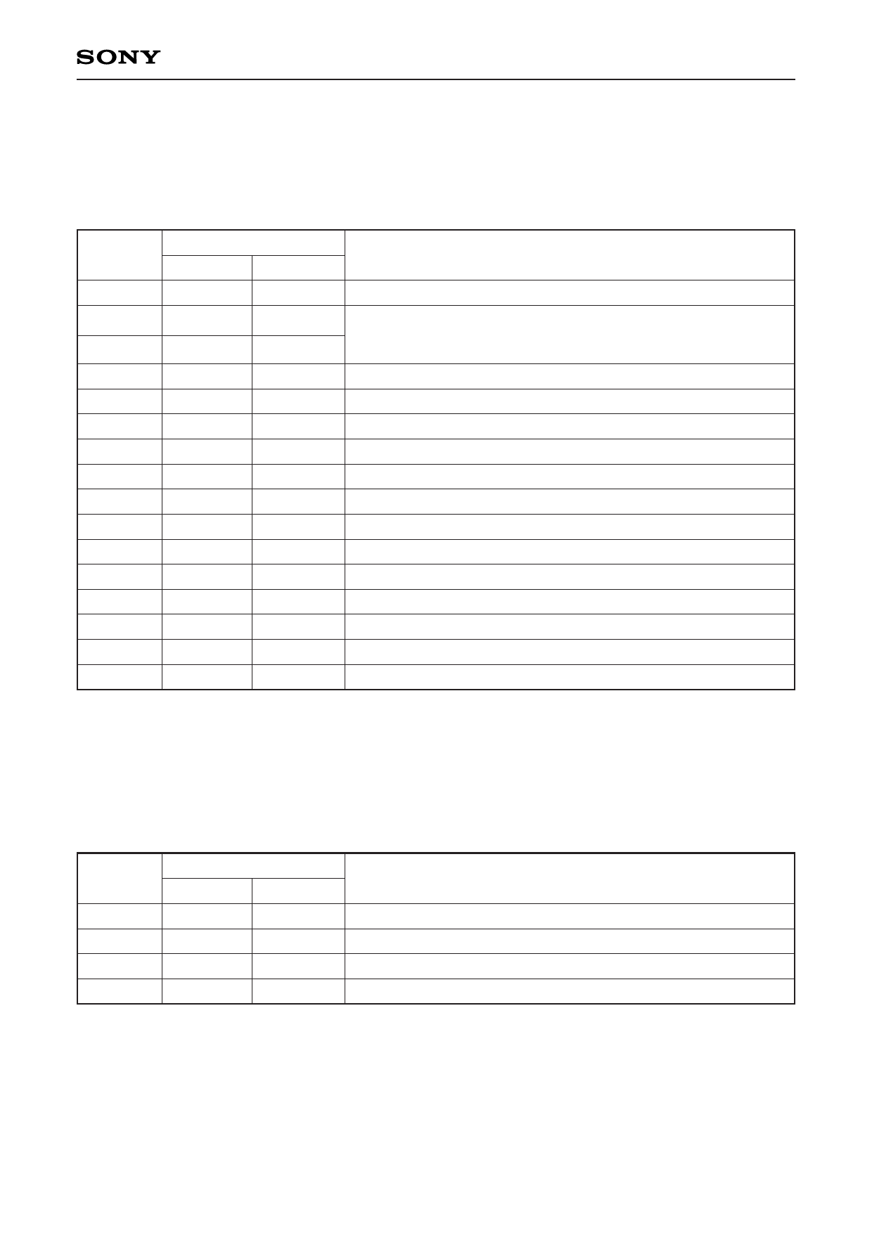
(6) Port setting
When the power turns on or initialization setting is performed by the reset input, the system starts operation
according to the selected port setting. Perform initialization after the setting is changed because the setting
can not be changed during operation.
I/O
Port
For reset For operation
Description
0
I
I
Test pin (Low = Normal mode)
1
I
2
I
I
Communication format selection
PORT[2:1] = (00: Sony Binary, 01: NMEA4800,
I
10: NMEA9600, 11: Unused)
3
I
I
RTC selection (High = Internal / Low = External)
4
I
I
Test pin (High = Normal mode)
5
I
I
Test pin (Low = Normal mode)
6
I
O
Unused
7
I
O
Unused
8
I
O
Unused
9
I
I
Antenna sense (Low = Disable / High = Enable)
10
I
O
Antenna shutdown (High = Cut)
11
I
I
Test pin (Low = Normal mode)
12
I
O
Unused
13
I
I/O
RTC SIO (Leave open when the internal RTC is selected.)
14
I
O
RTC SCL (Leave open when the internal RTC is selected.)
15
I
O
RTC CE (Leave open when the internal RTC is selected.)
(7) A/D setting
The antenna sense function can be realized by connecting the antenna power supply of the GPS receiver to
the A/D channel pins shown below. See the Application Circuit for the resistance value and others. See the
Port setting for the antenna sense function disable/enable selection.
I/O
VIN
For reset For operation
Description
0
I
I
Antenna power supply (before current value detection resistor)
1
I
I
Antenna power supply (after current value detection resistor)
2
I
I
Test pin (Low level fixed)
3
I
I
Test pin (Low level fixed)
– 17 –
Share Link: 