CXD2931GA-9 Просмотр технического описания (PDF) - Sony Semiconductor
Номер в каталоге
Компоненты Описание
производитель
CXD2931GA-9 Datasheet PDF : 27 Pages
| |||
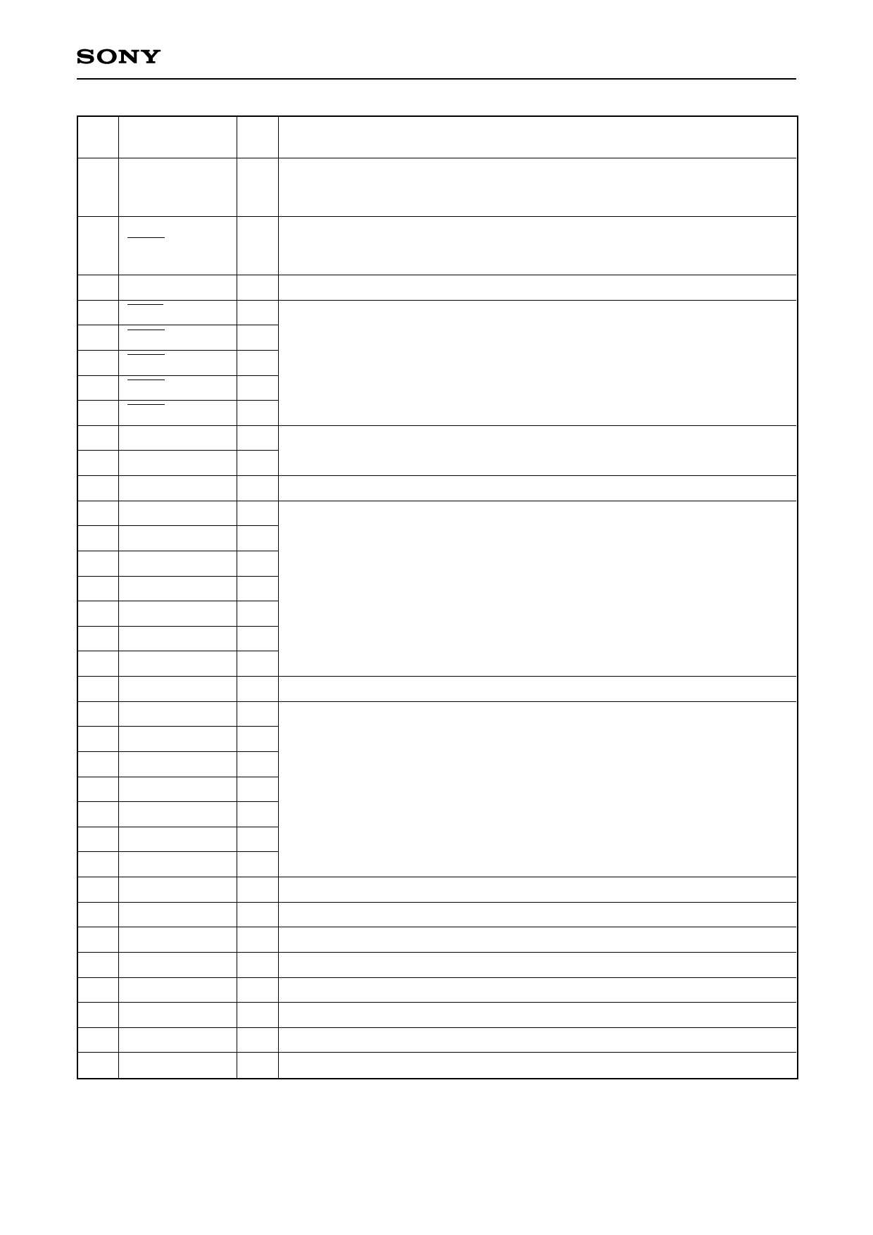
CXD2931R-9/GA-9
Pin
No.
Symbol
I/O
Description
111 SINT/PORT22
External interrupt input signal/general-purpose I/O port.
I/O This pin can be used as a general-purpose I/O port according to the internal
registers.
Chip select for external expansion data memory/general-purpose I/O port.
112 DCS0/PORT21 I/O This pin can be used as a general-purpose I/O port according to the internal
registers.
113 VDD
— Power supply.
114 DCS1/PORT20 I/O
115 DCS2/PORT19 I/O Chip select for external expansion data memory/general-purpose I/O port.
116 DCS3/PORT18 I/O These pins can be used as a general-purpose I/O port according to the
117 DCS4/PORT17 I/O internal registers.
118 DCS5/PORT16 I/O
119 PORT15
120 PORT14
I/O
General-purpose I/O port.
I/O
121 Vss
— GND
122 PORT13
I/O
123 PORT12
I/O
124 PORT11
I/O
125 PORT10
I/O General-purpose I/O port.
126 PORT9
I/O
127 PORT8
I/O
128 PORT7
I/O
129 VDD
— Power supply.
130 PORT6
I/O
131 PORT5
I/O
132 PORT4
I/O
133 PORT3
I/O General-purpose I/O port.
134 PORT2
I/O
135 PORT1
I/O
136 PORT0
I/O
137 Vss
— GND
138 TXD2
O UART transmission data output. (channel 2)
139 RXD2
I UART reception data input. (channel 2)
140 TXD1
O UART transmission data output. (channel 1)
141 RXD1
I UART reception data input. (channel 1)
142 TXD0
O UART transmission data output. (channel 0)
143 RXD0
I UART reception data input. (channel 0)
144 VDD
— Power supply.
–9–
Share Link: 