CXD2931GA-9 Просмотр технического описания (PDF) - Sony Semiconductor
Номер в каталоге
Компоненты Описание
производитель
CXD2931GA-9 Datasheet PDF : 27 Pages
| |||
CXD2931R-9/GA-9
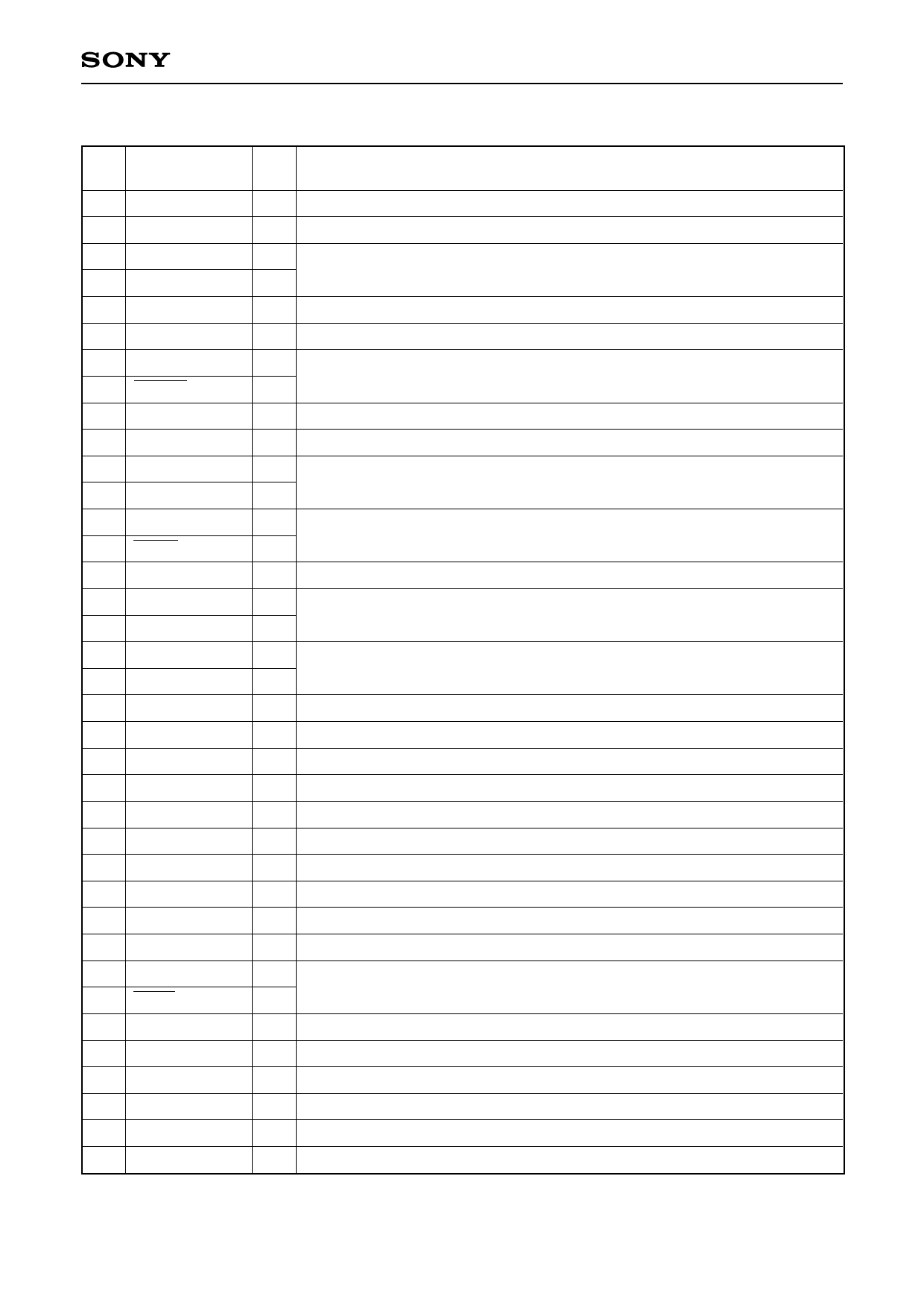
Pin Configuration
Pin
No.
Symbol
1 AVD
2 AVIN
3 VRT
4 VRB
5 AVS
6 Vss
7 TCXO
8 XTCXO
9 VDD
10 OTCXO
11 TEST0
12 TEST1
13 CCKI
14 CCKO
15 Vss
16 ICST0
17 ICST1
18 IF0
19 IF0O
20 TCXOS
21 VDD
22 HOLD
23 NMI
24 PMI
25 HOLDA
26 IODBK
27 EXRS
28 PWRST
29 Vss
30 CLKI
31 CLKO
32 CLKS
33 CLKOUT
34 VDD
35 RUN
36 IWR
37 IRD
I/O
Description
— A/D converter power supply.
I Analog input.
I
Reference input.
I
— A/D converter GND.
— GND
I
TCXO binary conversion circuit/crystal oscillator.
O
— Power supply.
O TCXO clock output.
I
Test. (Low level fixed)
I
I
Timer oscillation. (32.768kHz ± 100ppm)
O
— GND
I
Test. (Low level fixed)
I
I
IF signal binary conversion circuit.
O
I TCXO select. (Low: TCXO/2, High: TCXO through)
— Power supply.
I Hold input signal. (High: Hold)
I Non maskable interrupt.
I Program maskable interrupt.
O Hold acknowledge signal.
O Break signal for debugging.
I Reset input signal.
I Connect to main power supply. Leave open during backup.
— GND
I
CPU clock oscillation circuit.
O
I CPU clock select signal. (Low: TCXO, High: CLKI)
O CPU clock output.
— Power supply.
O Signal indicating CPU operating status.
O Write signal for external expansion memory.
O Read signal for external expansion memory.
–6–
Share Link: 