CXD2422R Просмотр технического описания (PDF) - Sony Semiconductor
Номер в каталоге
Компоненты Описание
производитель
CXD2422R Datasheet PDF : 22 Pages
| |||
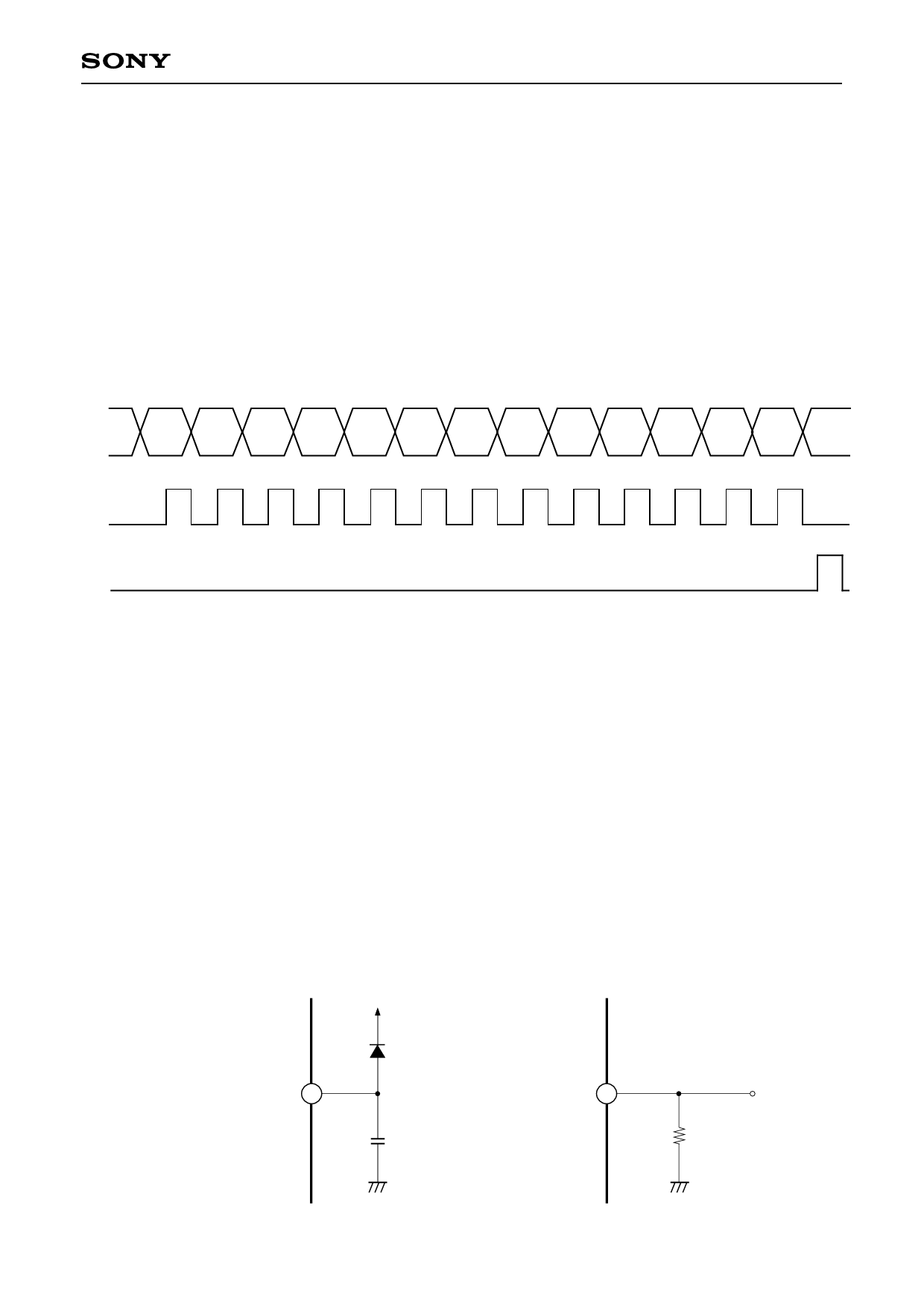
2) Inputting serial data
The accumulation time of the electronic shutter is controlled by external serial data.
Input pins (SD, SC, and LD) are used to input serial data.
SD: Serial data input
SC: Clock input
LD: Latch pulse input
The following is the serial data timing chart.
CXD2422R
SD
D3
D2
D1
D0
S8
S7
S6
S5
S4
S3
S2
S1
S0
SC
LD
D3 to D0: Not related to the accumulation time of the electronic shutter. Data are output to D3 to D0 pins
after converted into parallel data and being latched at LD.
S8 to S0: Sdata is set in 9-bit binary with S8 as MSB (High: 1, Low: 0). ON/OFF of the electronic shutter
and the accumulation time are determined by Sdata.
The calculation on the next page is for the accumulation time in each mode.
The data for SD are input to the internal 13-bit shift register, and the data can be retrieved as serial data at
SDO pin.
Note) The electronic shutter might operate from turning power on to inputting serial data. To prevent this
operation, process RST and LD pins as shown in the following figures. Be careful, however, as serial
data cannot be received before the voltage at RST rises.
VDD
RST 59
(with pull-up resistor)
LD 32
(with pull-up resistor)
1000p
4.7k
– 10 –
Share Link: 