CXD2400R Просмотр технического описания (PDF) - Sony Semiconductor
Номер в каталоге
Компоненты Описание
производитель
CXD2400R Datasheet PDF : 22 Pages
| |||
CXD2400R
External Synchronization
1) External/internal sync selection
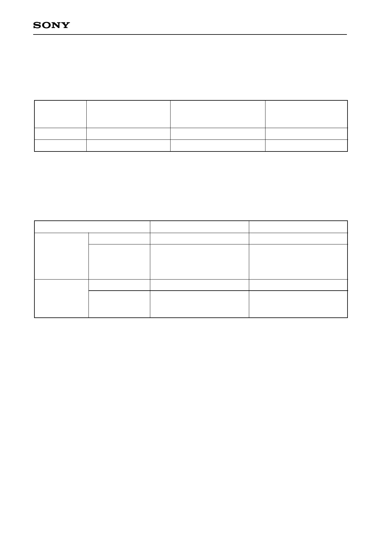
External or internal synchronization is selected automatically by a combination of 3 pins (VR/SYNC, HPLL and
ESYNC) to which the sync signal is input externally. The table below shows the input pattern combinations.
Input pattern
VR/SYNC pin: SYNC signal VR/SYNC pin: VD signal
VR/SYNC pin: Open
HPLL pin: Open
HPLL pin: HD signal
HPLL pin: Open
ESYNC pin: Open
ESYNC pin: VDD (power supply) ESYNC pin: Open
EXT pin output
High
High
Low
Sync state
External sync
External sync
Internal sync
Note) Operation is possible even if the VD cycle of the VD input in the VD/HD sync mode is longer than normal.
The EXT pin is the external/internal sync identification signal output pin. This output signal can be used as the
signal to select LC oscillation for expanding the lock range for external synchronization or the oscillator for
improving the oscillation accuracy for internal synchronization.
2) Modes for external synchronization
Field accumulation
Frame accumulation∗
Interlace
O
O
SYNC
synchronization Non-interlace
×
(Cannot be accomplished
since interlace operation
is the prior condition.)
×
(Cannot be accomplished
since interlace operation
is the prior condition.)
Interlace
O
O
VD/HD
synchronization Non-interlace
×
O
(Not practically applicable since
the sensitivity is halved.)
∗ The characteristics of CCD image sensors are guaranteed for field accumulation operation.
3) Reset operation
SYNC synchronization
The VR1 signal component is extracted from the SYNC signal supplied externally and, for EIA, V reset is
performed so that the VDO pulse falls at the count of 259H (262.5 – 3.5H) from the fall of the VR1 pulse. For
CCIR, it is reset in such a way that the VDO pulse falls at the count of 309H (312.5 – 3.5H). For these reasons,
it is a prerequisite that the SYNC signal input comply with the EIA or CCIR standard.
VD/HD synchronization
V reset is performed so that the VDO pulse falls 1H later after detecting the fall of the VD (VDR) pulse supplied
externally. Therefore, this enables V reset operation regardless of the field line number. The phase difference
between the VDR pulse and HDO pulse which is locked horizontally at PLL circuit identifies whether the field is
odd or even. (VDR must have a pulse width of 2H or more.)
– 11 –
Share Link: 