CXA1829N Просмотр технического описания (PDF) - Sony Semiconductor
Номер в каталоге
Компоненты Описание
производитель
CXA1829N Datasheet PDF : 15 Pages
| |||
CXA1829N
Description of Functions
Read amplifier
This is a low-noise amplifier for amplifying the faint signals from the heads, and is an emitter follower output. It
outputs the signals differentially to the RDX and RDY pins, and the X side of the head and RDX pin and the Y
side of the head and RDY pin have the same polarity. RDX and RDY outputs in Write mode become high
impedance. (The outputs should be capacitor-coupled.)
Write circuit
The Write data input to the WDI pin passes through a T flip-flop where its frequency is halved. It then drives
the Write switch circuit and supplies the Write current to the heads.
The Write data is triggered at the transition from high to low and the Write current is switched.
The Write current flows from the X side when the mode changes from Read to Write.
Mode control
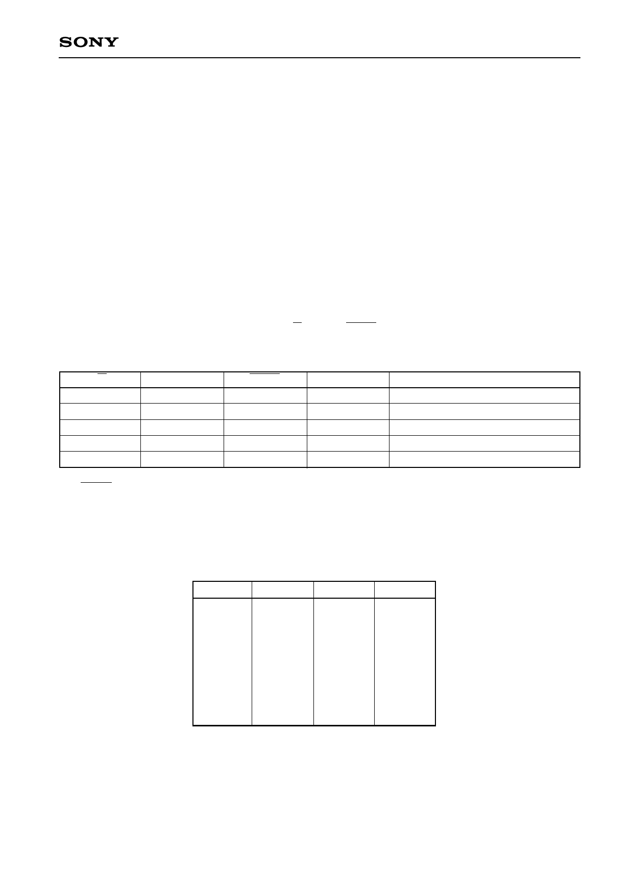
The modes are set as shown in Table 1 by the R/W, PS and WSER pins.
Table 1. Mode selection
R/W
PS
WSER
HSO
L
L
H
X
H
L
H
X
X
H
X
X
X
L
L
L
X
L
L
H
The WSER pin has a built-in pull-up resistor (100 kΩ).
Mode
Write
Read
Power save
0, 2, 4, 6-head simultaneous Write
1, 3, 5, 7-head simultaneous Write
Head selection
The heads are selected as shown in Table 2 by the HS0, HS1 and HS2 pins.
Table 2. Head selection
HS0
HS1
HS2
Head
L
L
L
0
H
L
L
1
L
H
L
2
H
H
L
3
L
L
H
4
H
L
H
5
L
H
H
6
H
H
H
7
—10—
Share Link: 