CXA1599Q Просмотр технического описания (PDF) - Sony Semiconductor
Номер в каталоге
Компоненты Описание
производитель
CXA1599Q Datasheet PDF : 23 Pages
| |||
CXA1599Q
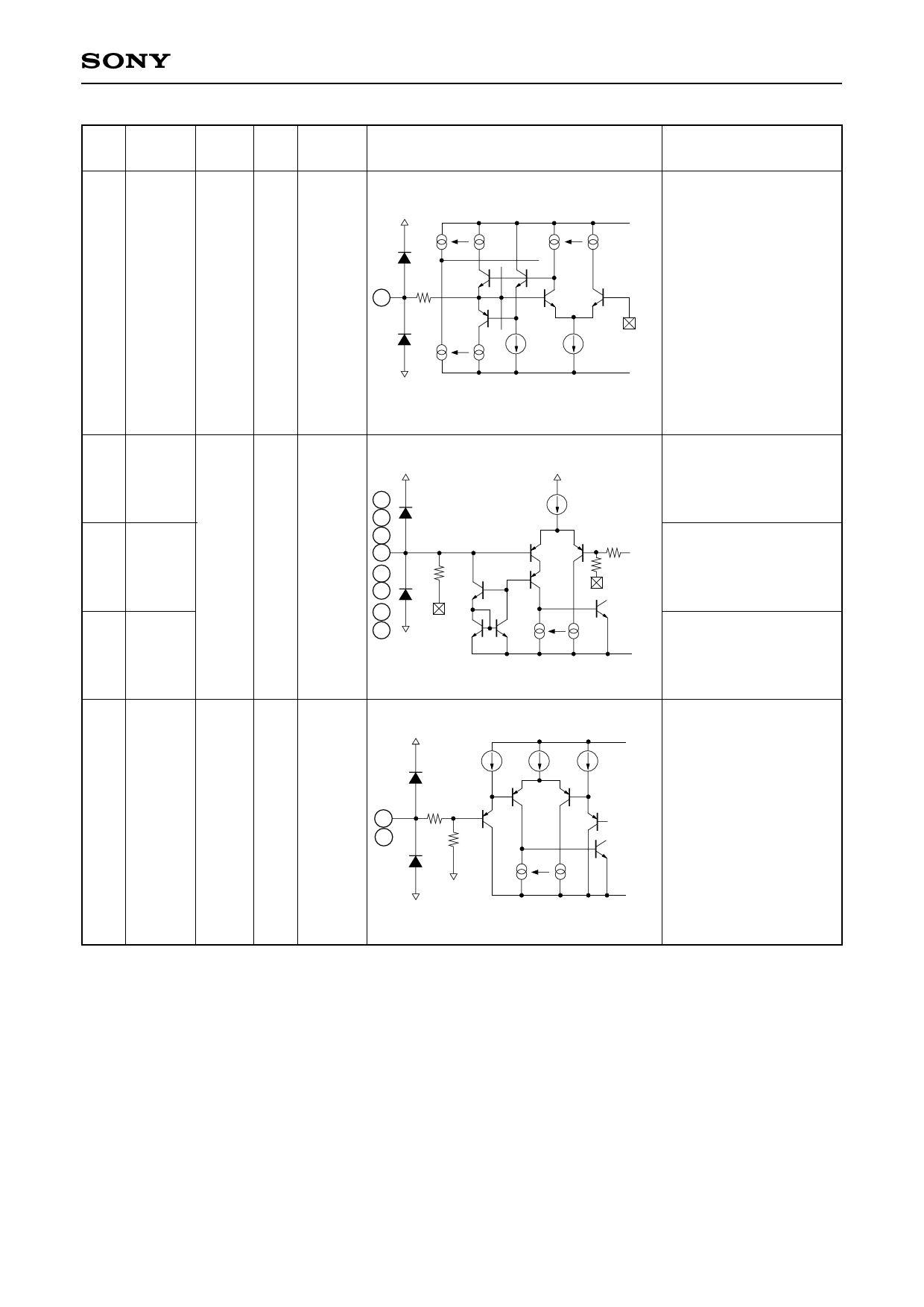
Pin
No.
Symbol
DC
voltage
I/O
I/O
resistance
Equivalent circuit
VCC
5
REC
CAL
2.5V
(During I
OPEN)
54kΩ
5
54k
×3
VEE
6 PB INB1
7 PB INB2
VCC
VCC
8 PB INA1
9 PB INA2
6
7
8
37 REC IN2
48 REC IN1 0.0V
I
9
50kΩ 37 50k
48
38 NR IN2
47 NR IN1
38
47
VEE
VGS
Description
VCC
DREF
VEE
Calibration for overall
frequency gain of
recording equalizer
amplifier.
Controls by applying the
DC voltage of DGND to
DVcc.
High → Gain up
Low → Gain down
∗When recording
calibration function is
not used, keep this pin
open.
Input of playback
equalizer amplifier.
Input of recording
VGS
equalizer amplifier.
Input pin for connecting
VEE Dolby line (decode)
output signal.
VCC
10 HP
VOL
33 REC
VOL
0.0V
(During I
OPEN)
100kΩ 10
33
60k
40k
×8
DGND
VEE
VCC Pin 10: Control for
headphone volume
Pin 33: Control for
recording volume
Controls by applying
the DC voltage of
DGND to DVcc for
each pin.
High → Volume up
VEE Low → Volume down
–4–
Share Link: 