CUS03(2013) Просмотр технического описания (PDF) - Toshiba
Номер в каталоге
Компоненты Описание
производитель
CUS03 Datasheet PDF : 5 Pages
| |||
TOSHIBA Schottky Barrier Rectifier Schottky Barrier Type
CUS03
CUS03
Switching Mode Power Supply Applications
Portable Equipment Battery Applications
• Forward voltage: VFM = 0.52 V@IF = 0.7 A
• Average forward current: IF (AV) = 0.7 A
• Repetitive peak reverse voltage: VRRM = 40 V
• Suitable for high-density board assembly due to the use of a small
surface-mount package, US−FLATTM
Absolute Maximum Ratings (Ta = 25°C)
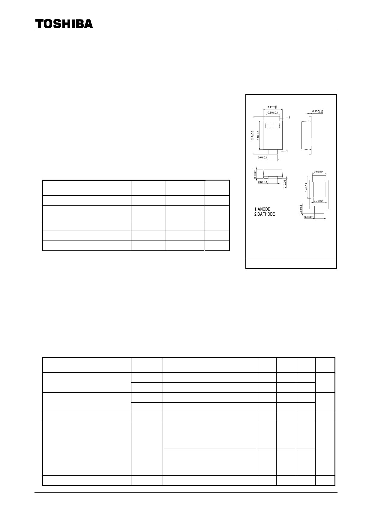
1.25
+ 0.2
− 0.1
0.88 ± 0.1
②
Unit: mm
0.13
+
−
0.05
0.03
①
0.6 ± 0.1
Characteristics
Symbol
Rating
Unit
0.88 ± 0.1
Repetitive peak reverse voltage
VRRM
40
V
0.6 ± 0.1
Average forward current
Peak one cycle surge forward current
(Non-repetitive)
Junction temperature
Storage temperature range
IF (AV)
IFSM
Tj
Tstg
0.7
(Note 1)
A
20 (50 Hz)
A
−40 to 150
°C
−40 to 150
°C
① ANODE
② CATHODE
0.78 ± 0.1
0.6 ± 0.1
Note 1: Ta = 53°C:
Device mounted on a glass-epoxy board
Board size: 50 mm × 50 mm,
Land size: 6 mm × 6 mm
Rectangular waveform (α = 180°), VR = 20 V
JEDEC
JEITA
TOSHIBA
―
―
3-2B1A
Note 2:
Using continuously under heavy loads (e.g. the application of
Weight: 0.004 g (typ.)
high temperature/current/voltage and the significant change in
temperature, etc.) may cause this product to decrease in the reliability significantly even if the operating
conditions (i.e. operating temperature/current/voltage, etc.) are within the absolute maximum ratings.
Please design the appropriate reliability upon reviewing the Toshiba Semiconductor Reliability Handbook
(“Handling Precautions”/“Derating Concept and Methods”) and individual reliability data (i.e. reliability test
report and estimated failure rate, etc).
Electrical Characteristics (Ta = 25°C)
Characteristics
Peak forward voltage
Repetitive peak reverse current
Junction capacitance
Thermal resistance
(junction to ambient)
Thermal resistance (junction to lead)
Symbol
Test Condition
Min Typ. Max Unit
VFM (1)
VFM (2)
IRRM (1)
IRRM (2)
Cj
Rth (j-a)
Rth (j-ℓ)
IFM = 0.1 A
―
IFM = 0.7 A
―
VRRM = 5 V
―
VRRM = 40 V
―
VR = 10 V, f = 1.0 MHz
―
Device mounted on a ceramic board
(board size: 50 mm × 50 mm)
(soldering land: 2 mm × 2 mm)
―
(board thickness: 0.64 mm)
Device mounted on a glass-epoxy board
(board size: 50 mm × 50 mm)
(soldering land: 6 mm × 6 mm)
―
(board thickness: 1.6 mm)
Junction to lead of cathode side
―
0.37 ―
V
0.48 0.52
0.4
―
μA
3.0 100
45
―
pF
―
75
°C/W
―
150
―
30 °C/W
Start of commercial production
2003-11
1
2013-11-01
Share Link: 