CMX869E2 Просмотр технического описания (PDF) - CML Microsystems Plc
Номер в каталоге
Компоненты Описание
производитель
CMX869E2 Datasheet PDF : 46 Pages
| |||
Low Power V.32 bis Modem
CMX869
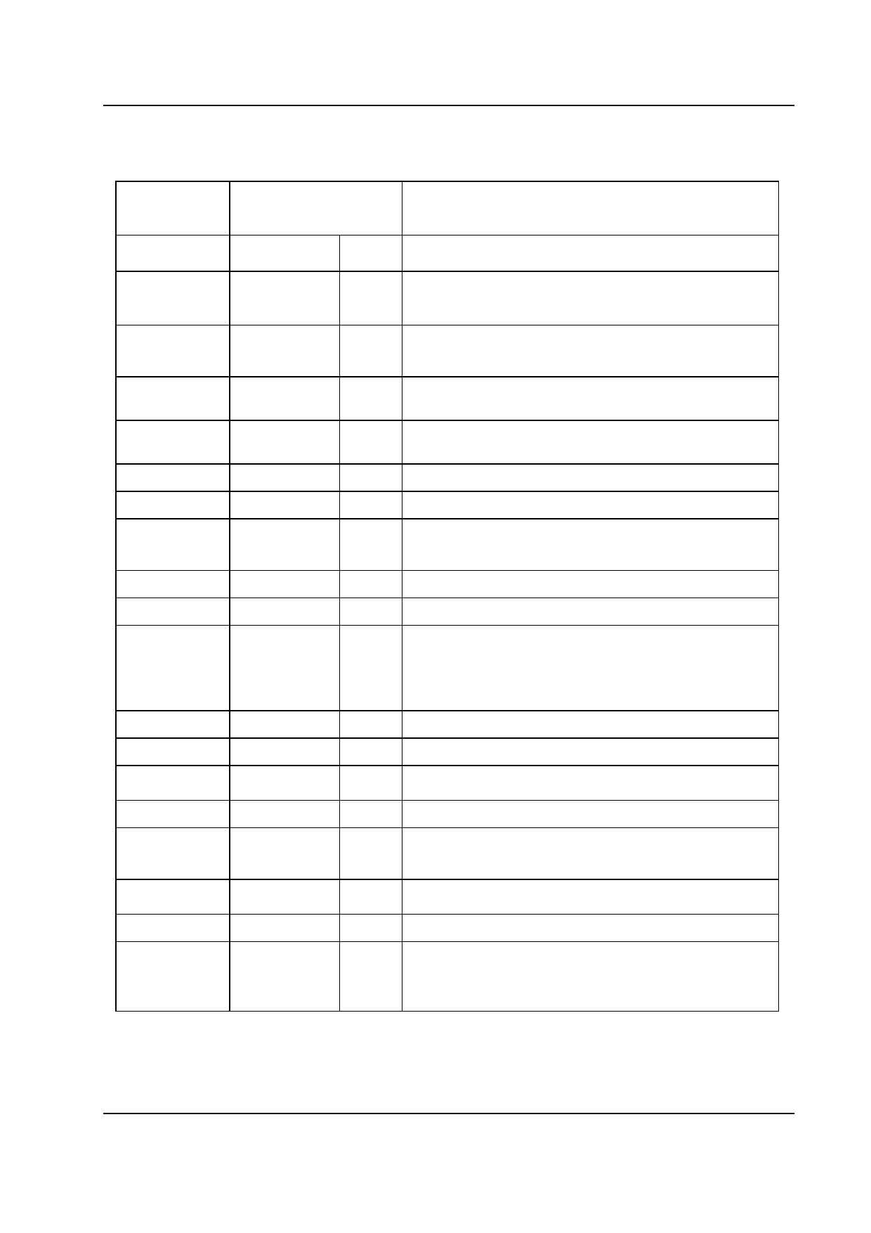
3. Signal List
CMX869
D2/E2/P4
Pin No.
1
2
4
5
6
8
9
10
11
13
14
15
17
18
20
21
22
24
Signal
Description
Name
REPLY DATA
RDRVN
SERIAL
CLOCK
COMMAND
DATA
CSN
RXA
RXBN
RXAN
RXAFB
VBIAS
TXAN
TXA
RDN
-
VDEC
XTAL/CLOCK
XTALN
IRQN
Type
TS
OP
IP
IP
IP
IP
IP
IP
OP
OP
OP
OP
IP
NC
PWR/
OP
IP
OP
OP
A 3-state C-BUS serial data output to the µC. This
output is high impedance when not sending data to the
µC.
Relay Drive output, low resistance pull down to VSS
when active and medium resistance pull up to VDD
when inactive.
The C-BUS serial clock input from the µC.
The C-BUS serial data input from the µC.
The C-BUS chip select input from the µC.
The non-inverting input to the Rx Input Amplifier
A second, switched inverting input to the Rx Input
Amplifier. Used to increase the input stage gain. If not
required, leave this pin unconnected.
The inverting input to the Rx Input Amplifier
The output of the Rx Input Amplifier.
Internally generated bias voltage of approximately
AVDD/2, except when the device is in ‘Powersave’
mode when VBIAS will discharge to AVSS. Must be
decoupled to AVSS by a capacitor mounted close to the
device pins.
The inverted output of the Tx Output Buffer.
The non-inverted output of the Tx Output Buffer.
Schmitt trigger input to the (inverting) Ring signal
detector. Connect to DVDD if Ring Detector is not used.
Reserved for future use. Do not connect to this pin.
Internally generated 2.5V supply voltage. Must be
decoupled to DVSS by capacitors mounted close to the
device pins. No other connections allowed.
The input to the oscillator inverter from the Xtal circuit
or external clock source.
The output of the on-chip Xtal oscillator inverter.
A ‘wire-ORable’ output for connection to a µC Interrupt
Request input. This output is pulled down to DVSS
when active and is high impedance when inactive. An
external pullup resistor is required ie R1 of Figure 2
© 2003 CML Microsystems Plc
4
D/869/1
Share Link: 