CMPWR330SA Просмотр технического описания (PDF) - California Micro Devices Corp
Номер в каталоге
Компоненты Описание
производитель
CMPWR330SA Datasheet PDF : 8 Pages
| |||
CALIFORNIA MICRO DEVICES
CMPWR330
Interface Signals
V is a positive input supply for the voltage regulator.
CC
Whenever this supply voltage exceeds the VCCSEL level
(4.4V), it will immediately be given priority and be used
to power the regulator output. If this supply voltage falls
below the VCCDES level (4.2V) it will immediately be
deselected and no longer provide power for the regula-
tor output. An internal hysteresis voltage of 0.2V is used
to prevent any chatter during selection and deselection
of VCC. The effective source impedance of VCC should be
kept below 0.3Ω to ensure changeover disturbances do
not exceed the hysteresis level.
If the connection to VCC is made within a few inches of
the main input filter, a bypass capacitor may not be
necessary. Otherwise a bypass filter capacitor in the
range of 1µF to 10µF will ensure adequate filtering.
VSBY is the standby input supply (5V), which is immedi-
ately used to power the regulator output whenever VCC is
below the deselect level (4.2V).
If the V connection is made within a few inches of the
SBY
main input filter, a bypass capacitor may not be neces-
sary. Otherwise a bypass filter capacitor in the range of
1µF to 10µF will ensure adequate filtering.
VAUX is the auxiliary voltage power source. This supply is
selected only when VCC falls below 4.2V and the VSBY is
not present. Under these conditions an internal switch is
enabled and provides a very low impedance connection
directly between VOUT and VAUX.
VOUT is the output voltage. Power is provided from the
regulator or via the low impedance auxiliary switch. This
output requires a capacitance of 10µF to ensure regula-
tor stability and minimize the peak output disturbance
during power supply changeover.
GND provides the reference for all voltages.
Pin
1
2
3
4
5-8
Symbol
VSYB
VCC
VOUT
VAUX
GND
INTERFACE SIGNALS
Description
Standby supply voltage (5V) input for regulator whenever VCC falls below 4.2V.
Primary supply voltage (5V) input for regulator
Regulator voltage output (3.3V) regulator when either VCC or VSYB is present
Auxiliary supply voltage (3.3V) input for low impedance switch
Reference for all voltages
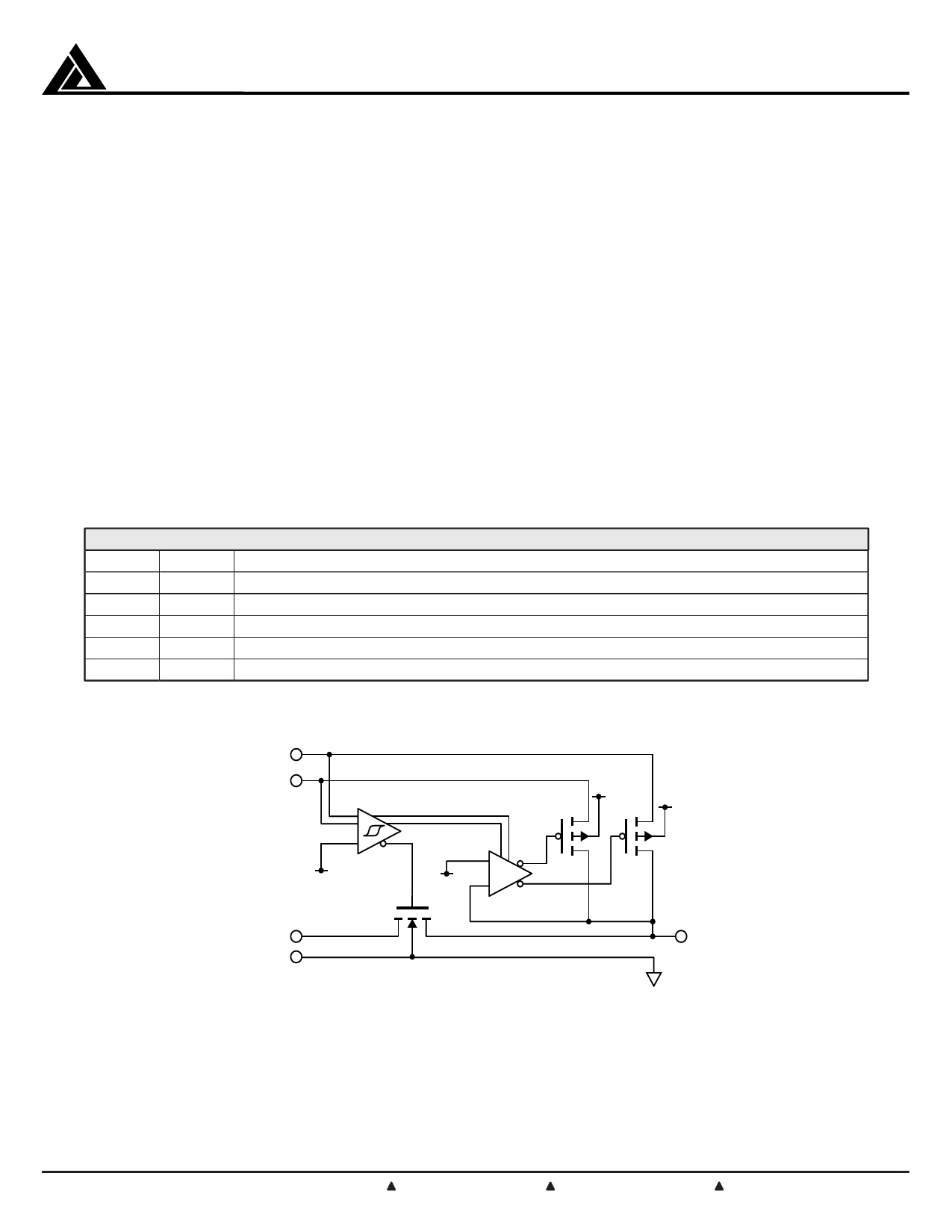
5VSBY
5VCC
CONTROLLER
+
+
–
AUXSW
VDESELECT
4.2V
AUXSW
0.25Ω
SELECT (VCC/VSBY)
ENABLE
VREF
3.3V
+
VCC
VSBY
–
REGULATOR AMP
3.3VAUX
GND
Simplified Electrical Schematic
VOUT
3.3V
400mA
GND
©2001 California Micro Devices Corp. All rights reserved. Smart OR™ is a trademark of California Micro Devices.
215 Topaz Street, Milpitas, California 95035 Tel: (408) 263-3214
Fax: (408) 263-7846
www.calmicro.com
3/6/2001
3
Share Link: 