CMPWR160SAR Просмотр технического описания (PDF) - California Micro Devices Corp
Номер в каталоге
Компоненты Описание
производитель
CMPWR160SAR Datasheet PDF : 10 Pages
| |||
CALIFORNIA MICRO DEVICES
CMPWR160
Interface Signals
VCC is the input power source for the Low Drop Out
Regulator, capable of delivering 3.3V/500mA output
current even when the input is as low as 4.2V.
Internal loading on this pin is typically 35µA when the
regulator is enabled, which reduces to only 7µA when-
ever the regulator is shutdown (SD taken Low). In the
event of VCC collapsing below VOUT, the loading at VCC will
immediately reduce to less than 0.1µA.
If the VCC pin is within a few inches of the main input
filter, a capacitor may not be necessary. Otherwise an
input filter capacitor in the range of 1µF to 10µF will
ensure adequate filtering.
SD is the regulator shutdown input logic signal which is
Active Low. This is a true CMOS input signal referenced
to VCC supply. When the pin is tied High (VCC ) the
regulator operates fully. When the pin is taken to GND,
the device enters shutdown mode and the regulator is
fully disabled. In this mode all critical POR circuitry
remains fully powered consuming less than 7µA (typical).
VOUT is the regulator output voltage used to power the
load. An output capacitor of 10µF is used to provide the
necessary phase compensation, thereby preventing
oscillation. The capacitor also helps to minimize the peak
output disturbance during line or load transients. When-
ever V collapses below the output the device immedi-
CC
ately enters reverse protection mode to prevent any
current flow back into the regulator pass transistor.
Under these conditions VOUT will also be used to provide
the necessary quiescent current for the internal refer-
ence and POR circuits. This ensures excellent start-up
characteristics for the regulator.
POR is the Power-On-Reset output pin (Active Low).
When VOUT rises above the POR threshold voltage
(typically 2.9V), the pin is forced to logic low (GND). The
pin remains logic low for 30ms then it is forced logic high
(3.3V). If VOUT falls below the POR threshold voltage
during this 30ms interval POR will remain logic low. If it
falls below the voltage threshold and then recovers the
30ms time will reset.
If VOUT falls below the POR threshold voltage POR is
immediately forced to logic low.
The power-on reset circuitry is designed to remain active
under all conditions and will produce a valid output even
when VCC is not present. A very low quiescent current
(7µA typical) ensures continuous operation of the POR
circuit.
GND is the negative reference for all voltages. This
current that flows in the ground connection is very low
(35µA typical with the regulator enabled and 7µA typical
with the regulator disabled).
Symbol
VCC
SD
POR
VOUT
GND
Pin Functions
Description
Positive supply input for regulator. When VCC falls below VOUT the regulator is disabled.
Shutdown control input signal (Active Low) to disable internal voltage regulator and current supply
to less than 7µA.
Power-On-Reset output signal is held Low until the output has been stable (>2.9V) for at least 30ms.
Regulator voltage ouput (3.3V) capable of delivering 500mA when device is enabled (SD is High).
Whenever the output exceeds 2.9V (TYP) the POR pulse is triggered.
Negative reference for all voltages
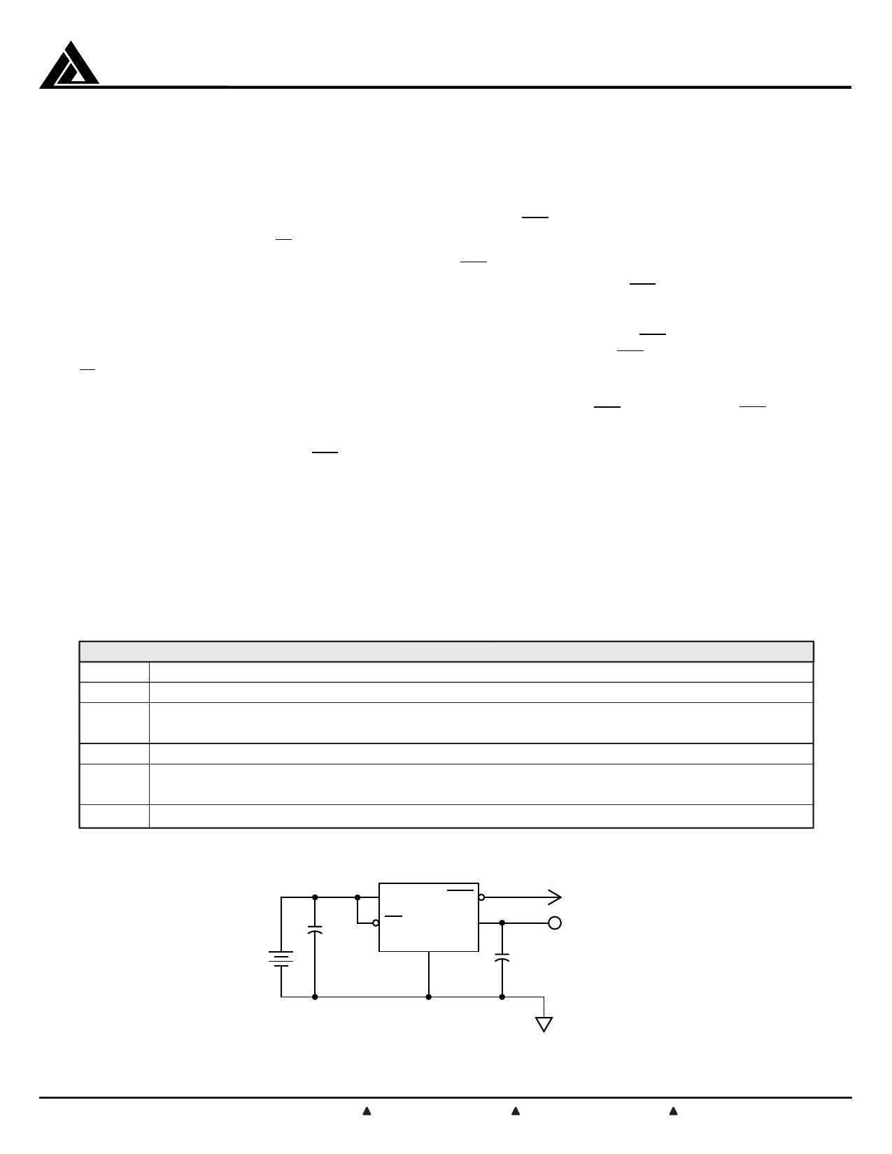
+ CIN
VCC
5V +
1µF
–
CMPWR160
VCC
POR
SD
VOUT
GND
+ COUT
10µF
uP Reset
VOUT
3.3V/500mA
GND
Typical Application Circuit
©2000 California Micro Devices Corp. All rights reserved. SmartOR™ is a trademark of California Micro Devices Corporation.
215 Topaz Street, Milpitas, California 95035 Tel: (408) 263-3214
Fax: (408) 263-7846
www.calmicro.com
12/5/2000
3
Share Link: 