CMPWR150TOR –ü—Ä–ĺ—Ā–ľ–ĺ—ā—Ä —ā–Ķ—Ö–Ĺ–ł—á–Ķ—Ā–ļ–ĺ–≥–ĺ –ĺ–Ņ–ł—Ā–į–Ĺ–ł—Ź (PDF) - California Micro Devices Corp
–Ě–ĺ–ľ–Ķ—Ä –≤ –ļ–į—ā–į–Ľ–ĺ–≥–Ķ
–ö–ĺ–ľ–Ņ–ĺ–Ĺ–Ķ–Ĺ—ā—č –ě–Ņ–ł—Ā–į–Ĺ–ł–Ķ
–Ņ—Ä–ĺ–ł–∑–≤–ĺ–ī–ł—ā–Ķ–Ľ—Ć
CMPWR150TOR Datasheet PDF : 8 Pages
| |||

CALIFORNIA MICRO DEVICES
CMPWR150
Interface Signals
VCC is the power source for the internal regulator and is
monitored continuously by an internal controller circuit.
Whenever VCC exceeds VCCSEL (4.35V typically), the internal
regulator (500mA max) will be enabled and deliver a fixed
3.3V at VOUT. When VCC falls below VCCDES (4.10V typically)
the regulator will be disabled
Internal loading on this pin is typically 1.0mA when the
regulator is enabled, which reduces to 0.15mA whenever
the regulator is disabled. If VCC falls below the voltage on
the VOUT pin the VCC loading will further reduce to only a
few microamperes.
During a VCC power up sequence, there will be an effective
step increase in VCC line current when the regulator is
enabled. The amplitude of this step increase will depend
on the dc load current and any necessary current required
for charging/discharging the load capacitance. This line
current transient will cause a voltage disturbance at the VCC
pin. The magnitude of the disturbance will be directly
proportional to the effective power supply source
impedance being delivered to the VCC input.
To prevent chatter during Select and Deselect transitions, a
built-in hysteresis voltage of 250mV has been incorporated.
It is recommended that the power supply connected to
the VCC input should have a source resistance of less than
0.25‚Ą¶ to minimize the event of chatter during the enabling/
disabling of the regulator.
An input filter capacitor in close proximity to the VCC pin
will reduce the effective source impedance and help
minimize any disturbances. If the VCC pin is within a few
inches of the main input filter, a capacitor may not be
necessary. Otherwise an input filter capacitor in the range
of 1uF to 10uF will ensure adequate filtering.
GND is the negative reference for all voltages. The current
that flows in the ground connection is very low (typically
1.0mA) and has minimal variation over all load conditions.
VOUT is the regulator output voltage connection used to
power the load. An output capacitor of ten microfarads is
used to provide the necessary phase compensation, thereby
preventing oscillation. The capacitor also helps to minimize
the peak output disturbance during power supply
changeover.
When VCC falls below VOUT, then VOUT will be used to provide
the necessary quiescent current for the internal reference
circuits. This ensures excellent start-up characteristics for
the regulator.
DRIVE is an active LOW logic output intended to be used
as the control signal for driving an external PFET whenever
the regulator is disabled. This will allow the voltage at VOUT
to be powered from an auxiliary supply voltage (3.3V).
The Drive pin is pulled HIGH to VCC whenever the regulator
is enabled. This ensures that the auxiliary remains isolated
during normal regulator operation.
n.c. pins are electrically isolated from the internal circuitry.
These pins can be connected to any external voltage level
without impacting the device funtionality.
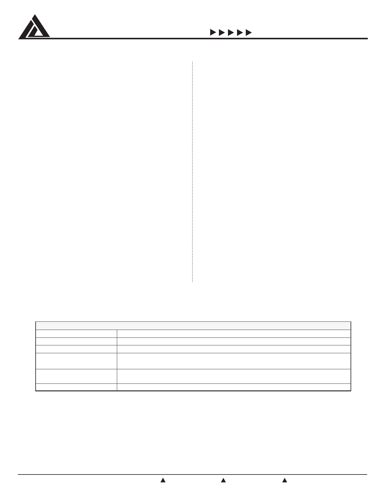
Symbol
VCC
GND
VO U T
Drive
n.c.
PIN FUNCTIONS
Description
Positive Supply input for regulator. When VCC falls below 4.1V, the regulator is disabled.
Negative reference for all voltages.
Regulator voltage output (3.3V) regulator when VCC is present. When VCC is not present, the
voltage on VOUT is used to bias the internal references.
CMOS Logic Output intended to control external PMOS switch for selecting an auxiliary
voltage supply when VCC is not present.
Unconnected pins which are electrically isolated from internal circuitry.
© 1999 California Micro Devices Corp. All rights reserved.
9/99
215 Topaz Street, Milpitas, California 95035 Tel: (408) 263-3214 Fax: (408) 263-7846 www.calmicro.com
3