CM1410 Просмотр технического описания (PDF) - ON Semiconductor
Номер в каталоге
Компоненты Описание
производитель
CM1410 Datasheet PDF : 10 Pages
| |||
CM1410
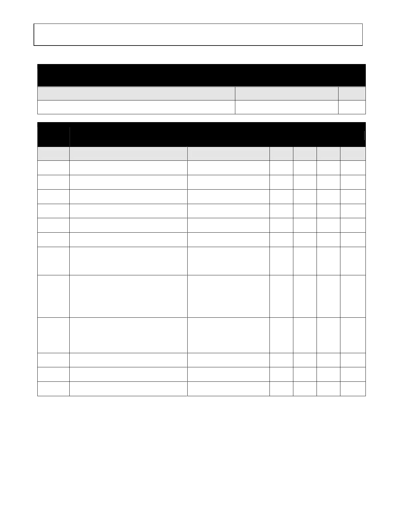
STANDARD OPERATING CONDITIONS
PARAMETER
Operating Temperature Range
RATING
-40 to +85
UNITS
°C
ELECTRICAL OPERATING CHARACTERISTICS (NOTE 1)
SYMBOL PARAMETER
R1
Resistance 1
R2
Resistance 2
R3
Resistance 3
C1
Capacitance 1
C2
Capacitance 2
ILEAK
Diode Leakage Current
VSIG
Signal Voltage
Positive Clamp
Negative Clamp
CONDITIONS
VIN=5.0V
ILOAD = 10mA
VESD In-system ESD Withstand Voltage
Notes 2 and 4
a) Human Body Model, MIL-STD-883,
Method 3015
b) Contact Discharge per IEC 61000-4-2
Level 4
VCL
Clamping Voltage during ESD Discharge Notes 2,3 and 4
MIL-STD-883 (Method 3015), 8kV
Positive Transients
Negative Transients
fC1
Cut-off frequency 1; Note 5
fC2
Cut-off frequency 2; Note 5
fC3
Cut-off frequency 3; Note 5
R = 100Ω, C = 47pF
R = 68Ω, C = 47pF
R = 10Ω, C = 100pF
MIN TYP MAX UNITS
90
100 110
Ω
61
68
75
Ω
9
10
11
Ω
38
47
57
pF
80
100 120
pF
1.0
µA
5
7
15
V
-15 -10
-5
V
±15
kV
±8
kV
+15
V
-19
V
53
MHz
61
MHz
33
MHz
Note 1: TA=25°C unless otherwise specified.
Note 2: ESD applied to input pins with respect to GND, one at a time, pins A2, A3, A4, B1 and B2 only.
Note 3: Clamping voltage is measured at the opposite side of the EMI filter to the ESD pin. For example, if ESD is applied to Pin
B1, then clamping voltage is measured at Pin C1.
Note 4: Unused pins are left open
Note 5: ZSOURCE=50Ω, ZLOAD=50Ω
Rev. 2 | Page 4 of 10 | www.onsemi.com
Share Link: 