CGY96 Просмотр технического описания (PDF) - Siemens AG
Номер в каталоге
Компоненты Описание
производитель
CGY96 Datasheet PDF : 10 Pages
| |||
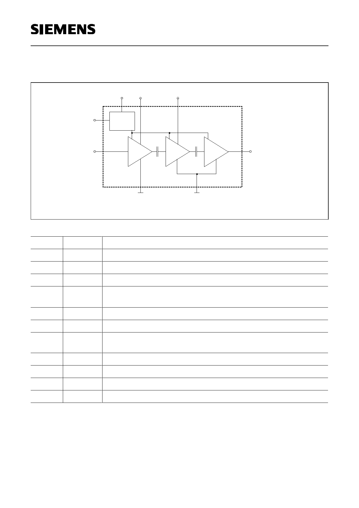
Functional block diagramm:
Vcontrol(8)
VD1(1)
Vneg(13)
current
control circuit
VD2(2)
RFin(16)
CGY 96
CGY96
VD3/RFout(4,5,6)
GND1(14,15)
GND2(17)
Pin #
1
2
3
4,5,6
7
8
9,10,11,
12
13
14,15
16
(17)
Name Configuration
VD1 Drain voltage 1st stage
VD2 Drain voltage 2nd stage
n.c. -
VD3 / Drain 3rd stage and RF-output
RFout
n.c. -
Vcontrol Control voltage for power ramping
n.c. -
Vneg
Gnd1
RFin
GND2
negative voltage for current control circuit
Ground pin 1st stage
RF Input
Ground (backside of MW16 package)
Siemens Aktiengesellschaft
2
Semiconductor Group
2
23.07.1998
HL HF19P9E8-G11a-A0s1
Share Link: 