CAT93C46R Просмотр технического описания (PDF) - Catalyst Semiconductor => Onsemi
Номер в каталоге
Компоненты Описание
производитель
CAT93C46R Datasheet PDF : 13 Pages
| |||
CAT93C46R
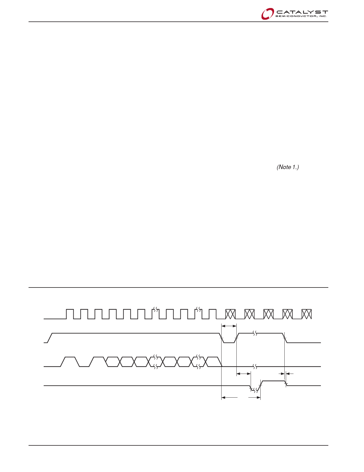
Write
After receiving a WRITE command, address and the
data, the CS (Chip Select) pin must be deselected for a
minimum of tCSMIN (see Design Note for details). The
falling edge of CS will start the self clocking clear and
data store cycle of the memory location specified in the
instruction. The clocking of the SK pin is not necessary
after the device has entered the self clocking mode.
The ready/busy status of the CAT93C46R can be
determined by selecting the device and polling the DO
pin. Since this device features Auto-Clear before write,
it is NOT necessary to erase a memory location before
it is written into.
Erase
Upon receiving an ERASE command and address, the
CS (Chip Select) pin must be deasserted for a minimum
of tCSMIN after the proper number of clock pulses (see
Design Note). The falling edge of CS will start the self
clocking clear cycle of the selected memory location.
The clocking of the SK pin is not necessary after the
device has entered the self clocking mode. The ready/
busy status of the CAT93C46R can be determined by
selecting the device and polling the DO pin. Once
cleared, the content of a cleared location returns to a
logical “1” state.
Erase All
Upon receiving an ERAL command, the CS (Chip Select)
pin must be deselected for a minimum of tCSMIN. The
falling edge of CS will start the self clocking clear cycle
of all memory locations in the device. The clocking of the
SK pin is not necessary after the device has entered the
self clocking mode. The ready/busy status of the
CAT93C46R can be determined by selecting the device
and polling the DO pin. Once cleared, the contents of all
memory bits return to a logical “1” state.
Write All
Upon receiving a WRAL command and data, the CS
(Chip Select) pin must be deselected for a minimum of
tCSMIN. The falling edge of CS will start the self clocking
data write to all memory locations in the device. The
clocking of the SK pin is not necessary after the device
has entered the self clocking mode. (Note 1.) The ready/
busy status of the CAT93C46R can be determined by
selecting the device and polling the DO pin. It is not
necessary for all memory locations to be cleared before
the WRAL command is executed.
Design Note
With CAT93C46R, after the last data bit has been
sampled, Chip Select (CS) must be brought Low before
the next rising edge of the clock(SK) in order to start the
slef-timed high voltage cycle. This is important because
if the CS is brought low before or after this specific frame
window, the addressed location will not be programmed
or erased.
Figure 4. Write Instruction Timing
SK
CS
AN AN-1
DI
101
A0 DN
HIGH-Z
DO
tCS MIN
STATUS
VERIFY
D0
STANDBY
tSV
BUSY
READY
tEW
tHZ
HIGH-Z
Doc. No. 1107, Rev. F
6
© 2006 by Catalyst Semiconductor, Inc.
Characteristics subject to change without notice
Share Link: 