CAT24C208 Просмотр технического описания (PDF) - Catalyst Semiconductor => Onsemi
Номер в каталоге
Компоненты Описание
производитель
CAT24C208 Datasheet PDF : 13 Pages
| |||
CAT24C208
I2C Bus Protocol
The following defines the features of the I2C bus protocol:
(1) Data transfer may be initiated only when the bus is
not busy.
(2) During a data transfer, the data line must remain
stable whenever the clock line is high. Any changes
in the data line while the clock line is high will be
interpreted as a START or STOP condition.
START Condition
The START Condition precedes all commands to the
device, and is defined as a HIGH to LOW transition of
either SDA when the respective SCL is HIGH. The
CAT24C208 monitors the SDA and SCL lines and will
not respond until this condition is met.
STOP Condition
A LOW to HIGH transition of SDA when SCL is HIGH
determines the STOP condition. All operations must end
with a STOP condition.
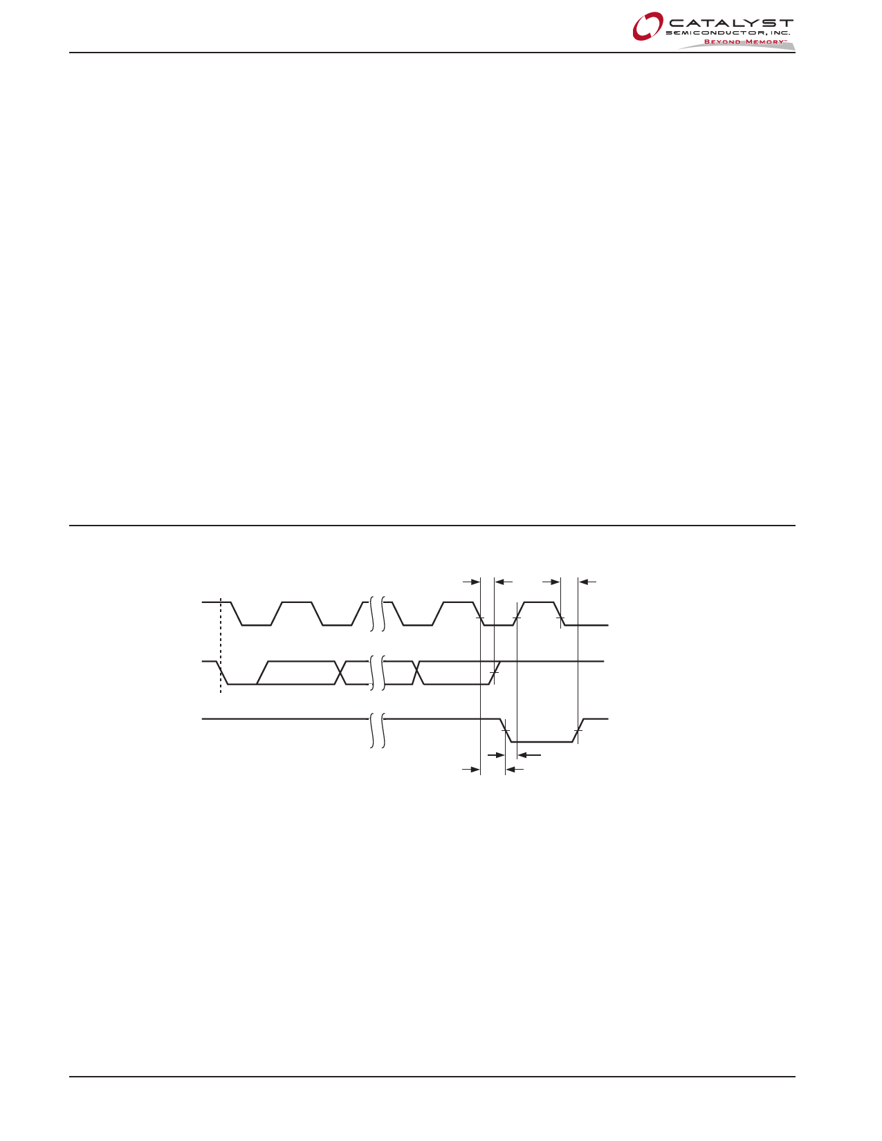
Acknowledge
After a successful data transfer, each receiving device is
required to generate an acknowledge. The acknowledging
device pulls down the respective SDA line during the ninth
clock cycle, signaling that it received the 8 bits of data.
The CAT24C208 responds with an acknowledge after
receiving a START condition and its slave address. If the
device has been selected along with a write operation, it
responds with an acknowledge after receiving each 8-bit
byte.
When the CAT24C208 is in a READ mode it transmits 8
bits of data, releases the respective SDA line, and
monitors the line for an acknowledge. Once it receives
this acknowledge, the CAT24C208 will continue to
transmit data. If no acknowledge is sent by the Master,
the device terminates data transmission and waits for a
STOP condition.
After an unsuccessful data transfer an acknowledge will
not be issued (NACK) by the slave (CAT24C208), and
the master should abort the sequence. If continued the
device will read from or write to the wrong address in the
two instruction format with the segment pointers.
Figure 2. Acknowledge Timing
SCL FROM
MASTER
BUS RELEASE DELAY (TRANSMITTER)
1
8
DATA OUTPUT
FROM TRANSMITTER
DATA OUTPUT
FROM RECEIVER
START
ACK DELAY
BUS RELEASE DELAY (RECEIVER)
9
ACK SETUP
Doc. No. 1044, Rev. F
6
© 2006 by Catalyst Semiconductor, Inc.
Characteristics subject to change without notice
Share Link: 