CAT24C208 Просмотр технического описания (PDF) - Catalyst Semiconductor => Onsemi
Номер в каталоге
Компоненты Описание
производитель
CAT24C208 Datasheet PDF : 13 Pages
| |||
CAT24C208
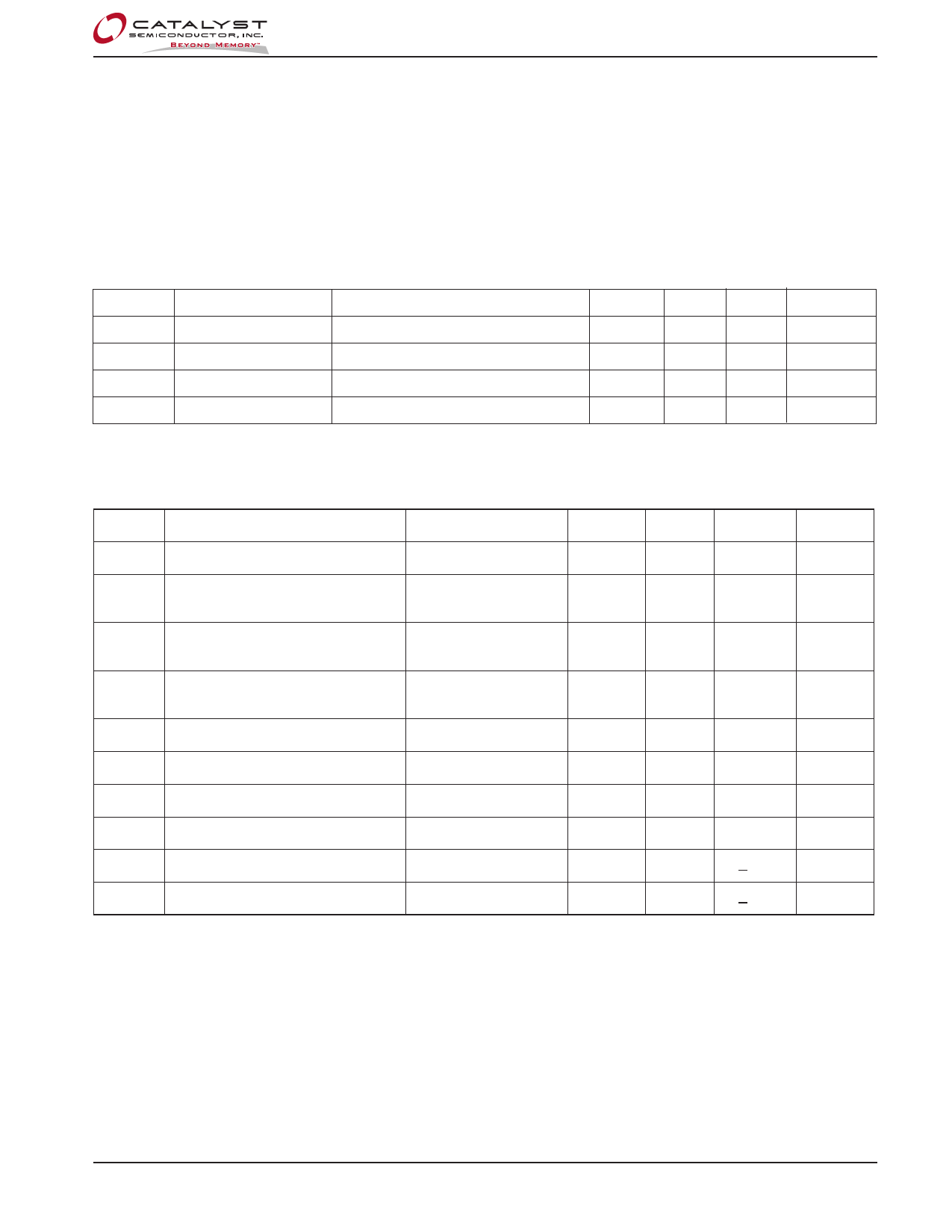
ABSOLUTE MAXIMUM RATINGS(1)
Temperature Under Bias .................. -55°C to +125°C
Storage Temperature ........................ -65°C to +150°C
Voltage on Any Pin with
Respect to Ground(2) ............ -2.0V to +VCC + 2.0V
VCC with Respect to Ground ................ -2.0V to +7.0V
Package Power Dissipation
Capability (TA = 25°C) ................................... 1.0W
Lead Soldering Temperature (10 secs) ............ 300°C
Output Short Circuit Current(3) ........................ 100mA
Reliability Characteristics
Symbol Parameter
NEND(4)
TDR(4)
VZAP(4)
ILTH(4)(5)
Endurance
Data Retention
ESD Susceptibility
Latch-up
Reference Test Method
Min
Typ
MIL-STD-883, Test Method 1033 1,000,000
MIL-STD-883, Test Method 1008 100
JEDEC Standard JESD 22
2000
JEDEC Standard 17
100
Max Units
Cycles/Byte
Years
Volts
mA
D.C. OPERATING CHARACTERISTICS
VCC = 2.5V to 5.5V, unless otherwise specified.
Symbol Parameter
Test Conditions
Min
Typ
Max
Units
ICC Power Supply Current
ISB Standby Current (VCC = 5.0V)
ILI Input Leakage Current
ILO Output Leakage Current
VIL
VIH
VHYS
Input Low Voltage
Input High Voltage
Input Hysteresis
fSCL = 100 KHz
VIN = GND or either
DSP or DDC VCC
VIN = GND to either
DSP or DDC VCC
VOUT = GND to either
DSP or DDC VCC
–1
VCC x 0.7
0.05
3
mA
50
µA
10
µA
10
µA
VCC x 0.3
V
VCC + 0.5
V
V
VOL1 Output Low Voltage (VCC = 3V)
IOL = 3 mA
0.4
V
VCCL1 Leakage DSP VCC to DDC VCC
+100
µA
VCCL2 Leakage DDC VCC to DSP VCC
+100
µA
Note:
(1) Stresses above those listed under “Absolute Maximum Ratings” may cause permanent damage to the device. These are stress ratings
only, and functional operation of the device at these or any other conditions outside of those listed in the operational sections of this
specification is not implied. Exposure to any absolute maximum rating for extended periods may affect device performance and reliability.
(2) The minimum DC input voltage is –0.5V. During transitions, inputs may undershoot to –2.0V for periods of less than 20 ns. Maximum DC
voltage on output pins is VCC +0.5V, which may overshoot to VCC + 2.0V for periods of less than 20ns.
(3) Output shorted for no more than one second. No more than one output shorted at a time.
(4) This parameter is tested initially and after a design or process change that affects the parameter.
(5) Latch-up protection is provided for stresses up to 100 mA on address and data pins from –1V to VCC +1V.
© 2006 by Catalyst Semiconductor, Inc.
Characteristics subject to change without notice
3
Doc No. 1044, Rev. F
Share Link: 