CAT24AA08WI-GT10 Просмотр технического описания (PDF) - ON Semiconductor
Номер в каталоге
Компоненты Описание
производитель
CAT24AA08WI-GT10 Datasheet PDF : 10 Pages
| |||
CAT24AA04, CAT24AA08
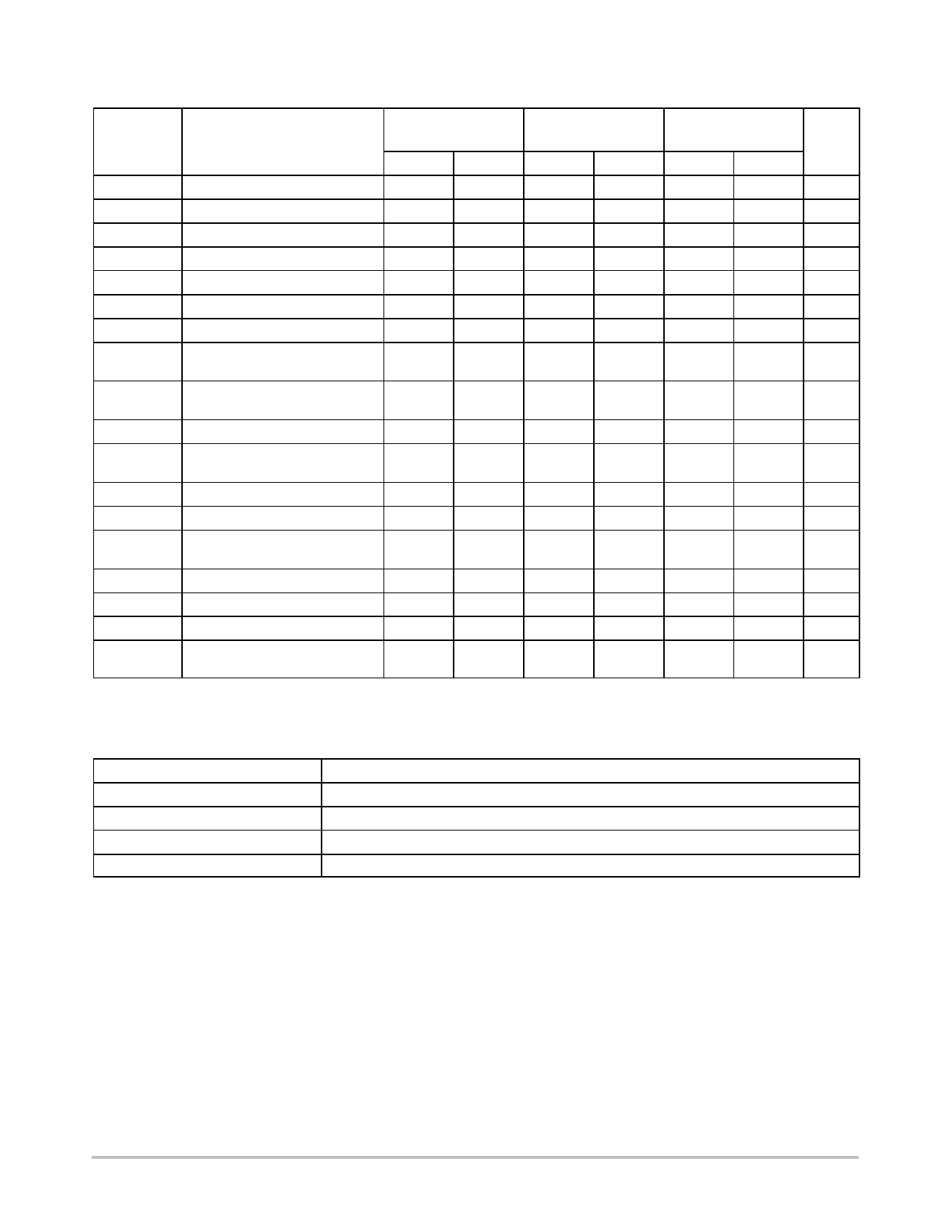
Table 5. A.C. CHARACTERISTICS (Note 5) (VCC = 1.7 V to 5.5 V, TA = −40°C to 85°C, unless otherwise specified.)
Standard
Fast
1 MHz
VCC = 1.7 V – 5.5 V
VCC = 1.7 V – 5.5 V
VCC = 2.5 V – 5.5 V
Symbol
Parameter
Min
Max
Min
Max
Min
Max
FSCL
Clock Frequency
100
400
1000
tHD:STA
START Condition Hold Time
4
0.6
0.25
tLOW
Low Period of SCL Clock
4.7
1.3
0.5
tHIGH
High Period of SCL Clock
4
0.6
0.5
tSU:STA
START Condition Setup Time
4.7
0.6
0.25
tHD:DAT
Data In Hold Time
0
0
0
tSU:DAT
Data In Setup Time
250
100
100
tR
(Note 6)
SDA and SCL Rise Time
1000
300
300
tF
(Note 6)
SDA and SCL Fall Time
300
300
100
tSU:STO
STOP Condition Setup Time
4
tBUF
Bus Free Time Between
4.7
STOP and START
0.6
0.25
1.3
0.5
tAA
tDH
Ti
(Note 6)
SCL Low to Data Out Valid
Data Out Hold Time
Noise Pulse Filtered at
SCL and SDA Inputs
3.5
0.9
0.4
100
50
50
100
100
100
tSU:WP
WP Setup Time
0
0
0
tHD:WP
tWR
tPU
(Notes 6, 7)
WP Hold Time
Write Cycle Time
Power−up to Ready Mode
2.5
2.5
1
5
5
5
1
1
1
5. Test conditions according to “A.C. Test Conditions” table.
6. Tested initially and after a design or process change that affects this parameter.
7. tPU is the delay between the time VCC is stable and the device is ready to accept commands.
Table 6. A.C. TEST CONDITIONS
Input Levels
Input Rise and Fall Times
Input Reference Levels
Output Reference Levels
Output Load
0.2 x VCC to 0.8 x VCC
≤ 50 ns
0.3 x VCC, 0.7 x VCC
0.5 x VCC
Current Source: IOL = 3 mA (VCC ≥ 2.5 V); IOL = 1 mA (VCC < 2.5 V); CL = 100 pF
Units
kHz
ms
ms
ms
ms
ns
ns
ns
ns
ms
ms
ms
ns
ns
ms
ms
ms
ms
http://onsemi.com
3
Share Link: 