CAT24AA01 Просмотр технического описания (PDF) - Catalyst Semiconductor => Onsemi
Номер в каталоге
Компоненты Описание
производитель
CAT24AA01 Datasheet PDF : 13 Pages
| |||
CAT24AA01, CAT24AA02
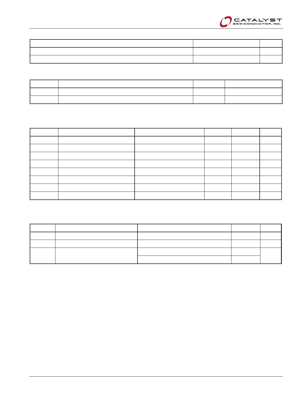
ABSOLUTE MAXIMUM RATINGS(1)
Parameters
Storage Temperature
Voltage on any Pin with Respect to Ground(2)
Ratings
–65 to +150
–0.5 to +6.5
Units
ºC
V
REABILITY CHARACTERISTICS(3)
Symbol
NEND(4)
TDR
Parameter
Endurance
Data Retention
Min
1,000,000
100
Units
Program/Erase Cycles
Years
D.C. OPERATING CHARACTERISTICS
VCC = 1.7 V to 5.5 V, TA = -40°C to 85°C, unless otherwise specified.
Symbol Parameter
Test Conditions
ICCR
ICCW
ISB
IL
VIL
VIH
VOL1
VOL2
Read Current
Write Current
Standby Current
I/O Pin Leakage
Input Low Voltage
Input High Voltage
Output Low Voltage
Output Low Voltage
Read, fSCL = 400 kHz
Write
All I/O Pins at GND or VCC
Pin at GND or VCC
VCC ≥ 2.5 V, IOL = 3.0 mA
VCC < 2.5 V, IOL = 1.0 mA
Min
-0.5
VCC x 0.7
Max
0.5
1
1
1
VCC x 0.3
VCC + 0.5
0.4
0.2
Units
mA
mA
μA
μA
V
V
V
V
PIN IMPEDANCE CHARACTERISTICS
VCC = 1.7 V to 5.5 V, TA = -40°C to 85°C, unless otherwise specified.
Symbol
CIN(3)
CIN(3)
IWP(5)
Parameter
SDA I/O Pin Capacitance
Input Capacitance (other pins)
WP Input Current
Conditions
VIN = 0V
VIN = 0V
VIN < VIH
VIN > VIH
Max
Units
8
pF
6
pF
100
μA
1
Notes:
(1) Stresses above those listed under “Absolute Maximum Ratings” may cause permanent damage to the device. These are stress ratings
only, and functional operation of the device at these or any other conditions outside of those listed in the operational sections of this
specification is not implied. Exposure to any absolute maximum rating for extended periods may affect device performance and reliability.
(2) The DC input voltage on any pin should not be lower than -0.5V or higher than VCC + 0.5V. During transitions, the voltage on any pin may
undershoot to no less than -1.5V or overshoot to no more than VCC + 1.5V, for periods of less than 20ns.
(3) These parameters are tested initially and after a design or process change that affects the parameter according to appropriate AEC-Q100
and JEDEC test methods.
(4) Page Mode @ 25°C
(5) When not driven, the WP pin is pulled down to GND internally. For improved noise immunity, the internal pull-down is relatively strong;
therefore the external driver must be able to supply the pull-down current when attempting to drive the input HIGH. To conserve power, as
the input level exceeds the trip point of the CMOS input buffer (~ 0.5 x VCC), the strong pull-down reverts to a weak current source.
Doc. No. MD-1120 Rev. B
2
© Catalyst Semiconductor, Inc.
Characteristics subject to change without notice
Share Link: 