CAT1021 Просмотр технического описания (PDF) - ON Semiconductor
Номер в каталоге
Компоненты Описание
производитель
CAT1021
ON Semiconductor

CAT1021 Datasheet PDF : 24 Pages
| |||
CAT1021, CAT1022, CAT1023
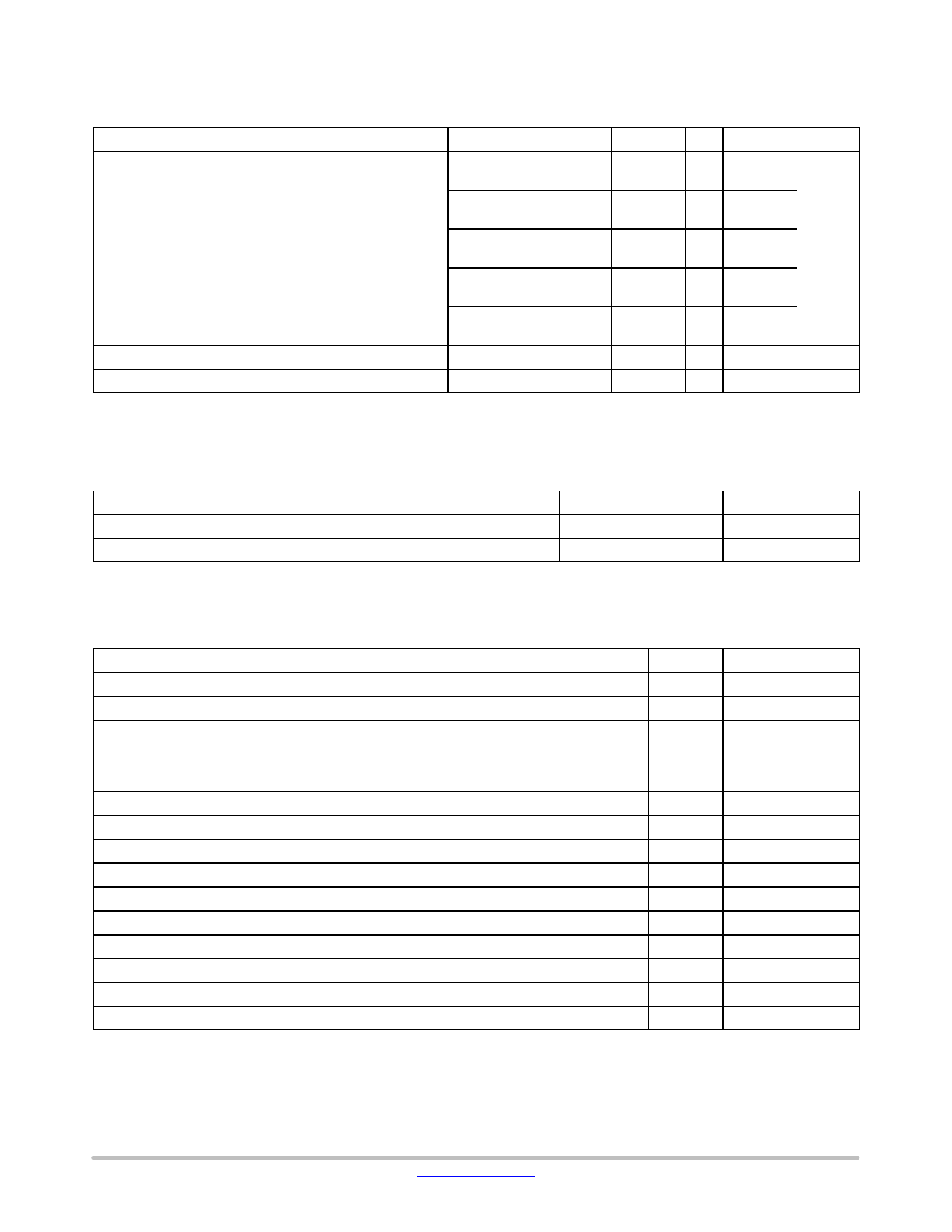
Table 6. D.C. OPERATING CHARACTERISTICS
VCC = 2.7 V to 5.5 V and over the recommended temperature conditions unless otherwise specified.
Symbol
Parameter
Test Conditions
Min
Typ Max
VTH
Reset Threshold
CAT102x−45
(VCC = 5.0 V)
4.50
4.75
CAT102x−42
(VCC = 5.0 V)
4.25
4.50
CAT102x−30
(VCC = 3.3 V)
3.00
3.15
CAT102x−28
(VCC = 3.3 V)
2.85
3.00
CAT102x−25
(VCC = 3.0 V)
2.55
2.70
VRVALID
Reset Output Valid VCC Voltage
1.00
VRT (Note 4) Reset Threshold Hysteresis
15
3. VIL min and VIH max are reference values only and are not tested.
4. This parameter is tested initially and after a design or process change that affects the parameter. Not 100% tested.
Table 7. CAPACITANCE
TA = 25°C, f = 1.0 MHz, VCC = 5 V
Symbol
Test
COUT (Note 5)
CIN (Note 5)
Output Capacitance
Input Capacitance
Test Conditions
VOUT = 0 V
VIN = 0 V
Max
8
6
Units
V
V
mV
Units
pF
pF
Table 8. AC CHARACTERISTICS
VCC = 2.7 V to 5.5 V and over the recommended temperature conditions, unless otherwise specified.
Memory Read & Write Cycle (Note 6)
Symbol
Parameter
Min
Max
Units
fSCL
Clock Frequency
400
kHz
tSP
Input Filter Spike Suppression (SDA, SCL)
100
ns
tLOW
Clock Low Period
1.3
ms
tHIGH
Clock High Period
0.6
ms
tR (Note 5)
SDA and SCL Rise Time
300
ns
tF (Note 5)
SDA and SCL Fall Time
300
ns
tHD; STA
Start Condition Hold Time
0.6
ms
tSU; STA
Start Condition Setup Time (for a Repeated Start)
0.6
ms
tHD; DAT
Data Input Hold Time
0
ns
tSU; DAT
Data Input Setup Time
100
ns
tSU; STO
Stop Condition Setup Time
0.6
ms
tAA
SCL Low to Data Out Valid
900
ns
tDH
Data Out Hold Time
50
ns
tBUF (Note 5) Time the Bus must be Free Before a New Transmission Can Start
1.3
ms
tWC (Note 7) Write Cycle Time (Byte or Page)
5
ms
5. This parameter is characterized initially and after a design or process change that affects the parameter. Not 100% tested.
6. Test Conditions according to “AC Test Conditions” table.
7. The write cycle time is the time from a valid stop condition of a write sequence to the end of the internal program/erase cycle. During the
write cycle, the bus interface circuits are disabled, SDA is allowed to remain high and the device does not respond to its slave address.
www.onsemi.com
5
Share Link: