CAT1021 Просмотр технического описания (PDF) - ON Semiconductor
Номер в каталоге
Компоненты Описание
производитель
CAT1021
ON Semiconductor

CAT1021 Datasheet PDF : 24 Pages
| |||
CAT1021, CAT1022, CAT1023
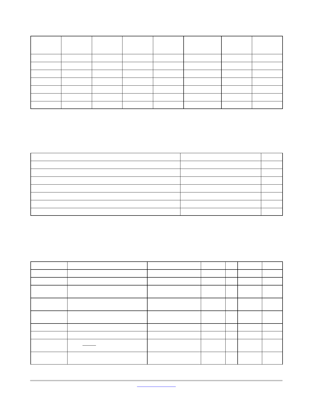
Table 4. CAT102X FAMILY OVERVIEW
Device
Manual Reset Watchdog
Input Pin
Watchdog
Monitor Pin
Write
Protection
Pin
Independent
Auxiliary Voltage
Sense
RESET:
Active High
and LOW
EEPROM
CAT1021
n
n
SDA
n
n
2k
CAT1022
n
n
SDA
2k
CAT1023
n
n
WDI
n
2k
CAT1024
n
2k
CAT1025
n
n
n
2k
CAT1026
n
n
2k
CAT1027
n
WDI
n
2k
NOTE: Device will meet the specifications after thermal equilibrium has been established when mounted in a test socket or printed circuit
board with maintained transverse airflow greater than 500 lfpm.
SPECIFICATIONS
Table 5. ABSOLUTE MAXIMUM RATINGS
Parameters
Ratings
Units
Temperature Under Bias
–55 to +125
°C
Storage Temperature
–65 to +150
°C
Voltage on any Pin with Respect to Ground (Note 1)
VCC with Respect to Ground
Package Power Dissipation Capability (TA = 25°C)
Lead Soldering Temperature (10 s)
−2.0 to VCC + 2.0
V
−2.0 to 7.0
V
1.0
W
300
°C
Output Short Circuit Current (Note 2)
100
mA
Stresses exceeding those listed in the Maximum Ratings table may damage the device. If any of these limits are exceeded, device functionality
should not be assumed, damage may occur and reliability may be affected.
1. The minimum DC input voltage is –0.5 V. During transitions, inputs may undershoot to –2.0 V for periods of less than 20 ns. Maximum
DC voltage on output pins is VCC +0.5 V, which may overshoot to VCC +2.0 V for periods of less than 20 ns.
2. Output shorted for no more than one second. No more than one output shorted at a time.
Table 6. D.C. OPERATING CHARACTERISTICS
VCC = 2.7 V to 5.5 V and over the recommended temperature conditions unless otherwise specified.
Symbol
Parameter
Test Conditions
Min
Typ
ILI
Input Leakage Current
VIN = GND to VCC
−2
ILO
Output Leakage Current
VIN = GND to VCC
−10
ICC1
Power Supply Current (Write)
fSCL = 400 kHz
VCC = 5.5 V
ICC2
Power Supply Current (Read)
fSCL = 400 kHz
VCC = 5.5 V
ISB
Standby Current
VCC = 5.5 V
VIN = GND to VCC
VIL (Note 3)
VIH (Note 3)
VOL
Input Low Voltage
Input High Voltage
Output Low Voltage
(SDA, RESET)
IOL = 3 mA
VCC = 2.7 V
−0.5
0.7 x VCC
VOH
Output High Voltage
(RESET)
IOH = −0.4 mA
VCC = 2.7 V
VCC − 0.75
Max
10
10
3
1
60
0.3 x VCC
VCC + 0.5
0.4
Units
mA
mA
mA
mA
mA
V
V
V
V
www.onsemi.com
4
Share Link: