CA3083(1998) Просмотр технического описания (PDF) - Intersil
Номер в каталоге
Компоненты Описание
производитель
CA3083 Datasheet PDF : 4 Pages
| |||
CA3083
Absolute Maximum Ratings
Thermal Information
The following ratings apply for each transistor in the device:
Collector-to-Emitter Voltage, VCEO . . . . . . . . . . . . . . . . . . . . . . 15V
Collector-to-Base Voltage, VCBO . . . . . . . . . . . . . . . . . . . . . . . . 20V
Collector-to-Substrate Voltage, VCIO (Note 1) . . . . . . . . . . . . . . 20V
Emitter-to-Base Voltage, VEBO . . . . . . . . . . . . . . . . . . . . . . . . . . 5V
Collector Current (IC) . . . . . . . . . . . . . . . . . . . . . . . . . . . . . . . 100mA
Base Current (IB) . . . . . . . . . . . . . . . . . . . . . . . . . . . . . . . . . . . 20mA
Operating Conditions
Temperature Range . . . . . . . . . . . . . . . . . . . . . . . . . -55oC to 125oC
Thermal Resistance (Typical, Note 2)
θJA (oC/W) θJC (oC/W)
PDIP Package . . . . . . . . . . . . . . . . . . . 135
N/A
SOIC Package . . . . . . . . . . . . . . . . . . . 200
N/A
Maximum Power Dissipation (Any One Transistor) . . . . . . . 500mW
Maximum Junction Temperature (Plastic Package) . . . . . . . 150oC
Maximum Storage Temperature Range . . . . . . . . . . -65oC to 150oC
Maximum Lead Temperature (Soldering 10s) . . . . . . . . . . . . 300oC
(SOIC - Lead Tips Only)
CAUTION: Stresses above those listed in “Absolute Maximum Ratings” may cause permanent damage to the device. This is a stress only rating and operation of the
device at these or any other conditions above those indicated in the operational sections of this specification is not implied.
NOTES:
1. The collector of each transistor of the CA3083 is isolated from the substrate by an integral diode. The substrate must be connected to a voltage
which is more negative than any collector voltage in order to maintain isolation between transistors and provide normal transistor action. To avoid
undesired coupling between transistors, the substrate Terminal (5) should be maintained at either DC or signal (AC) ground. A suitable bypass
capacitor can be used to establish a signal ground.
2. θJA is measured with the component mounted on an evaluation PC board in free air.
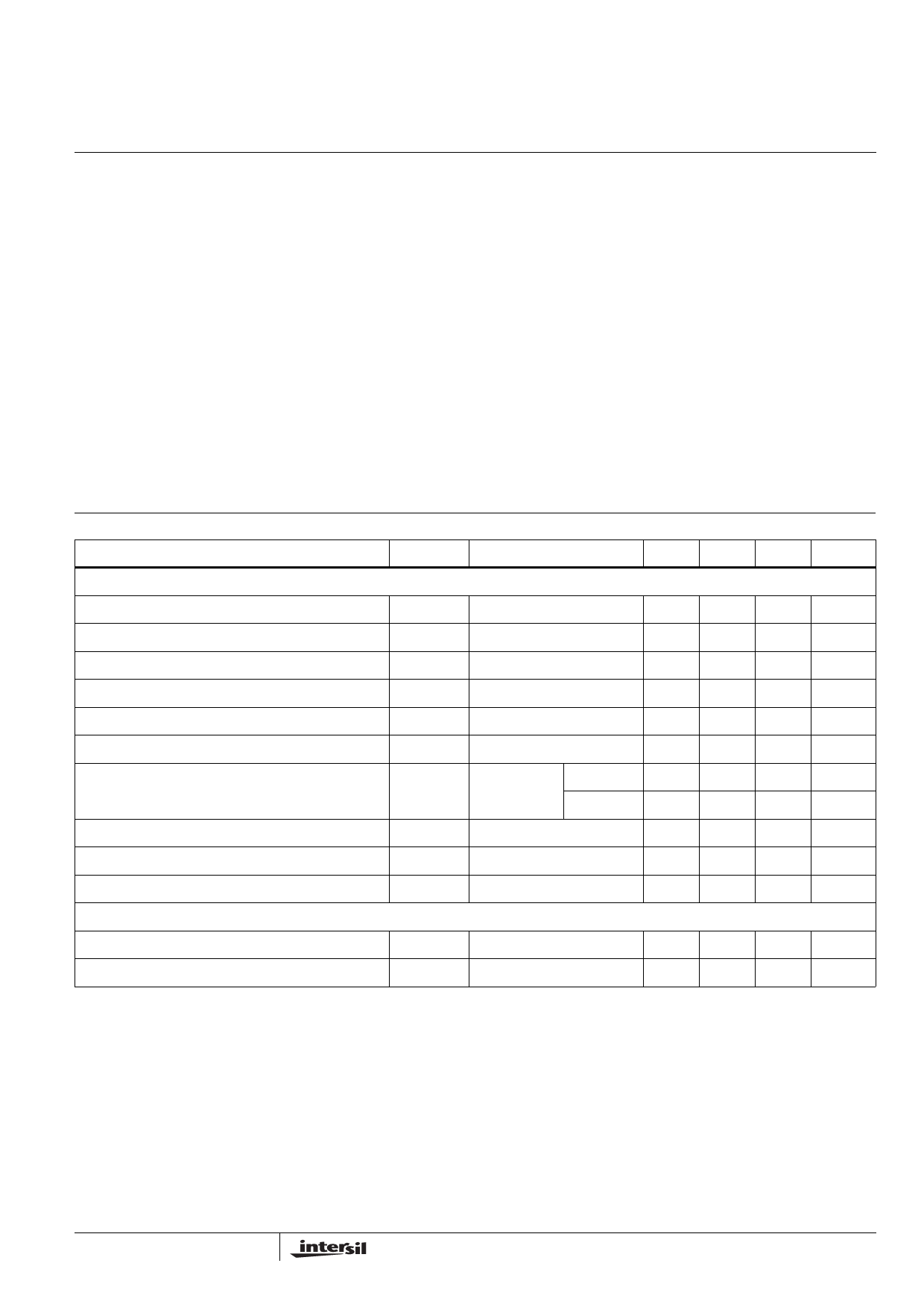
Electrical Specifications For Equipment Design, TA = 25oC
PARAMETER
SYMBOL
TEST CONDITIONS
MIN
TYP MAX UNITS
FOR EACH TRANSISTOR
Collector-to-Base Breakdown Voltage
V(BR)CBO IC = 100µA, IE = 0
20
Collector-to-Emitter Breakdown Voltage
V(BR)CEO IC = 1mA, IB = 0
15
Collector-to-Substrate Breakdown Voltage
V(BR)CIO ICI = 100µA, IB = 0, IE = 0
20
Emitter-to-Base Breakdown Voltage
V(BR)EBO IE = 500µA, IC = 0
5
Collector-Cutoff-Current
ICEO
VCE = 10V, IB = 0
-
Collector-Cutoff-Current
ICBO
VCB = 10V, IE = 0
-
DC Forward-Current Transfer Ratio (Note 3) (Figure 1)
hFE
VCE = 3V
IC = 10mA
40
IC = 50mA
40
Base-to-Emitter Voltage (Figure 2)
VBE
VCE = 3V, IC = 10mA
0.65
Collector-to-Emitter Saturation Voltage (Figures 3, 4)
VCE SAT IC = 50mA, IB = 5mA
-
Gain Bandwidth Product
fT
VCE = 3V, IC = 10mA
-
FOR TRANSISTORS Q1 AND Q2 (As a Differential Amplifier)
Absolute Input Offset Voltage (Figure 6)
|VIO|
VCE = 3V, IC = 1mA
-
Absolute Input Offset Current (Figure 7)
|IIO|
VCE = 3V, IC = 1mA
-
NOTE:
3. Actual forcing current is via the emitter for this test.
60
24
60
6.9
-
-
76
75
0.74
0.40
450
1.2
0.7
-
-
-
-
10
1
-
-
0.85
0.70
-
5
2.5
V
V
V
V
µA
µA
V
V
MHz
mV
µA
2
Share Link: 