UDA1344TS Просмотр технического описания (PDF) - Philips Electronics
Номер в каталоге
Компоненты Описание
производитель
UDA1344TS Datasheet PDF : 28 Pages
| |||
Philips Semiconductors
Low-voltage low-power stereo audio
CODEC with DSP features
Product specification
UDA1344TS
FUNCTIONAL DESCRIPTION
The UDA1344TS accommodates slave mode only, this
means that in all applications the system devices must
provide the system clock. The system clock must be
locked in frequency to the digital interface input signals.
The BCK clock can be up to 128fs, or in other words the
BCK frequency is 128 times the Word Select (WS)
frequency or less: fBCK = < 128 × fWS.
Remarks:
1. The WS edge MUST fall on the negative edge of the
BCK clock at all times for proper operation of the digital
I/O data interface
2. The sampling frequency range is from 8 to 55 kHz
3. For MSB- and LSB-justified formats it is important to
have a WS signal with a duty factor of 50%.
Analog-to-Digital Converter (ADC)
The stereo ADC of the UDA1344TS consists of two
3rd-order Sigma-Delta modulators. They have a modified
Ritchie-coder architecture in a differential switched
capacitor implementation. The oversampling ratio is 128.
In contrast to the UDA1340M, the UDA1344TS supports
1 V (RMS) input signals and can be set, via an external
resistor, to support 2 V (RMS) input signals.
Analog front-end
The analog front-end is equipped with a selectable 0 dB or
6 dB gain block. The pin to select the gain switch is given
in Section “L3 mode”. This block can be used in
applications in which both 1 V (RMS) and 2 V (RMS) input
signals are available.
In applications in which a 2 V (RMS) input signal is used,
a 12 kΩ resistor must be connected in series with the input
of the ADC. This makes a voltage divider with the internal
ADC resistor and makes sure only 1 V (RMS) maximum is
input to the IC. Using this application for a 2 V (RMS) input
signal, the gain switch must be set to 0 dB. When a
1 V (RMS) input signal is input to the ADC in the same
application, the gain switch must be set to 6 dB.
An overview of the maximum input voltages allowed
against the presence of an external resistor and the setting
of the gain switch is given in Table 1.
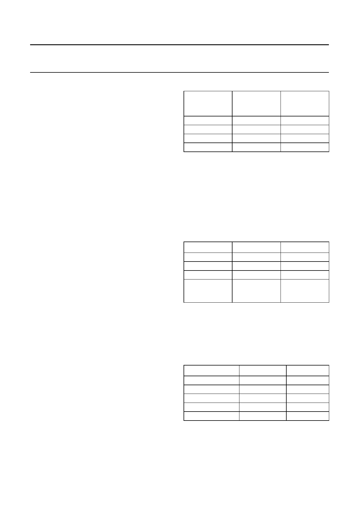
Table 1 Application modes using input gain stage
RESISTOR
(12 kΩ)
Present
Present
Absent
Absent
INPUT GAIN
SWITCH
0 dB
6 dB
0 dB
6 dB
MAXIMUM
INPUT
VOLTAGE
2 V (RMS)
1 V (RMS)
1 V (RMS)
0.5 V (RMS)
Decimation filter (ADC)
The decimation from 128fs to 1fs is performed in 2 stages.
The first stage realizes 3rd-order s----i-nx-----x- characteristic. This
filter decreases the sample rate by 16.
The second stage, a Finite Impulse Response (FIR) filter,
consists of 3 half-band filters, each decimating by a factor
of 2.
Table 2 Decimation filter characteristics
ITEM
Pass-band ripple
Stop band
Dynamic range
Overall gain with
0 dB input to the
ADC
CONDITIONS
0 − 0.45fs
>0.55fs
0 − 0.45fs
DC
VALUE (dB)
±0.05
−60
108
−1.16
DC-cancellation filter (ADC)
An optional Infinite Impulse-Response (IIR) high-pass filter
is provided to remove unwanted DC components.
The operation is selected by the microcontroller via the
L3 interface. The filter characteristics are given in Table 3.
Table 3 DC-cancellation filter characteristics
ITEM
Pass-band ripple
Pass-band gain
Droop
Attenuation at DC
Dynamic range
CONDITIONS
−
−
at 0.00045fs
at 0.00000036fs
0 − 0.45fs
VALUE (dB)
none
0
0.031
>40
>110
2001 Jun 29
6
Share Link: 