PBL40309 Просмотр технического описания (PDF) - Ericsson
Номер в каталоге
Компоненты Описание
производитель
PBL40309 Datasheet PDF : 6 Pages
| |||
PBL 403 09
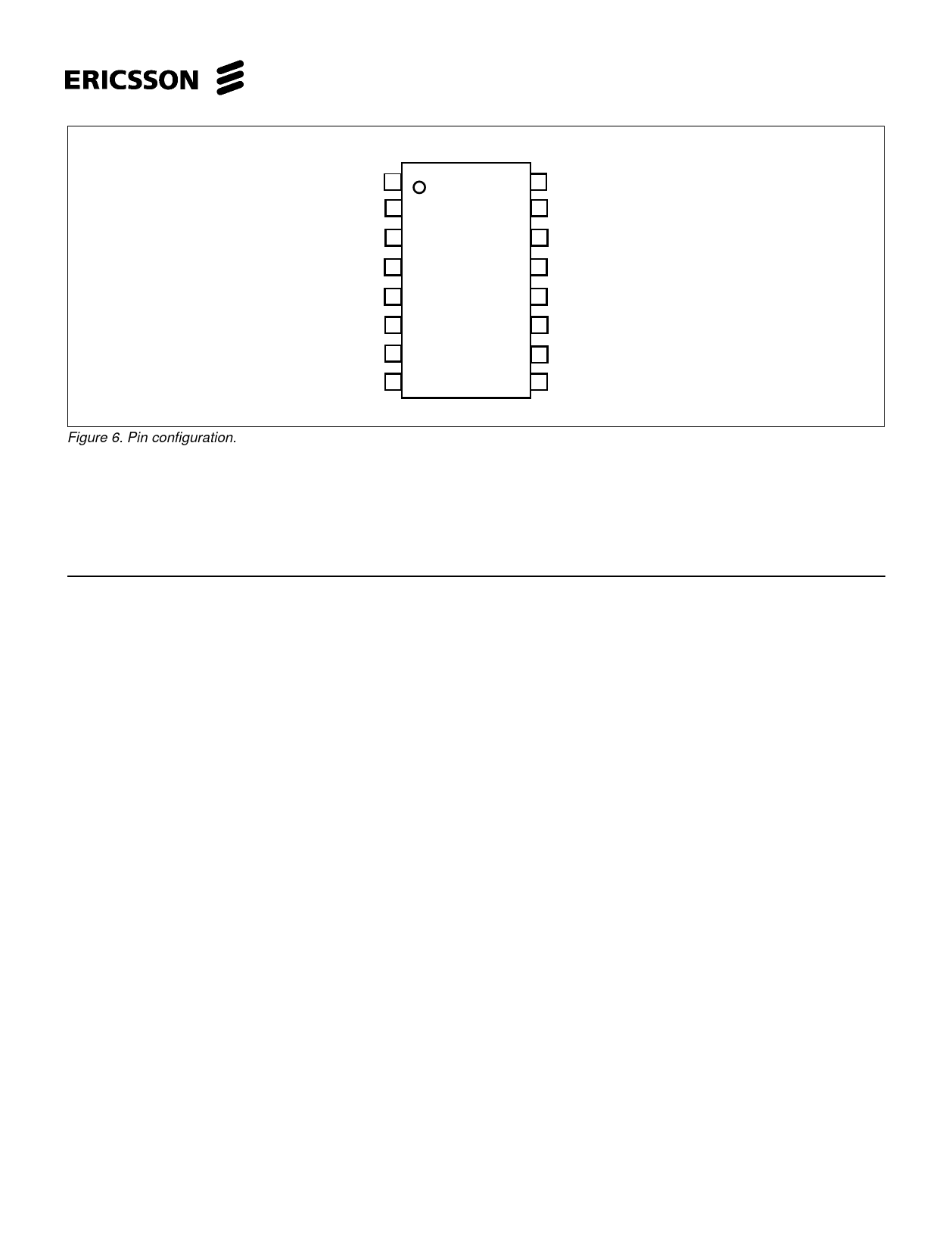
Figure 6. Pin configuration.
PA-ON 1
GND 2
RFinA 3
GND 4
GND 5
RFinB 6
GND 7
Vcc 8
Pin Descriptions:
Refer to pin configuration.
SO Name
Function
1 PA-ON
2 GND
3 RFinA
4 GND
5 GND
6 RFinB
7 GND
8 Vcc
PA On/Off Control pin (active low)
Common ground
RF input
Common ground
Common ground
RF input
Common ground
Supply voltage
16 GND
15 GND
14 RFoutA
13 GND
12 GND
11 RFoutB
10 GND
9 GND
SO Name
Function
9 GND
10 GND
11 RFoutB
12 GND
13 GND
14 RFoutA
15 GND
16 GND
Common ground
Common ground
RF output
Common ground
Common ground
RF output
Common ground
Common ground
Functional description.
PBL403 09 is a differential two stage integrated power amplifier intended for DECT. The circuit is manufactured in a bipolar 5.0 V
technology with additional features for improved wireless performance. Input and interstage matching is done completely on-chip,
tuned to 1.9 GHz, and only normal supply decoupling plus output matching is necessary. If the device is used in a single ended
environment, input and output transformers need to be added to the external circuitry.
PBL403 09 is optimized to work at a supply voltage of 3.6 V, but is able to operate between 2.7 and 5.2 V. At 3.6 V it can deliver up
to 31 dBm when driven into compression, while 27 dBm is guaranteed with an input power of 4 dBm. Best Power Added Efficiency
(PAE) is obtained close to maximum output power where PAE exeeds 50 %. Small signal gain is 25-26 dB. In a DECT handset with
the duty cycle 1/24, the average power dissipation in the circuit is low, normally between 30 to 40 mW. In the base station, the duty
cycle can increase and PBL403 09 can be operated at CW with a small penalty in power gain and output power (< 0.5 dB).
Operation is controlled through a power-on pin which is active low. When active, the current consumption is typically 135 mA without
any input signal present. When not active, current consumption is less than 10 µA.
3
Share Link: 