VN16117L1 Просмотр технического описания (PDF) - Vaishali Semiconductor
Номер в каталоге
Компоненты Описание
производитель
VN16117L1 Datasheet PDF : 15 Pages
| |||
VN16117
Preliminary
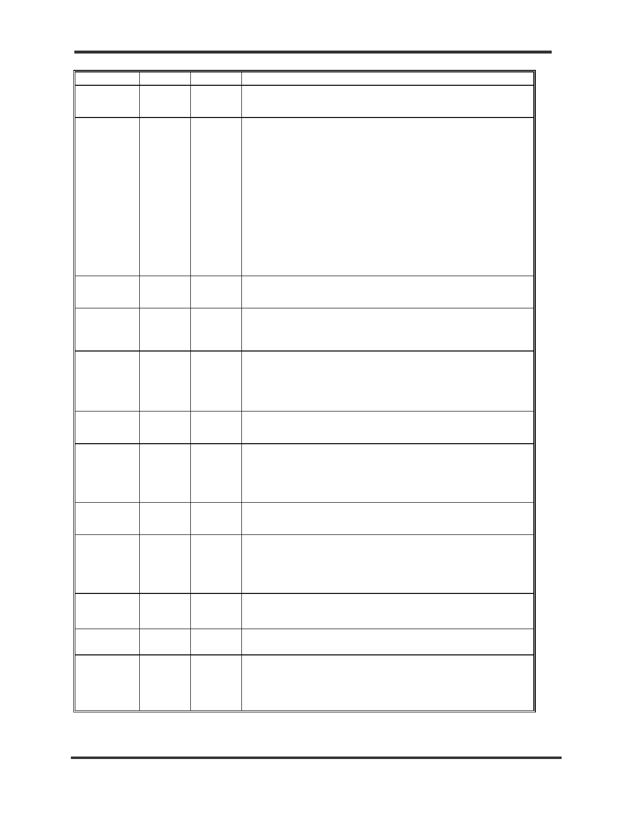
Table 1. Pin Description
Name
GND_ESD
VCC_ESD
Pin #
1, 14
5, 10
Type
Power
Description
Power and ground pairs for pad ESD structure.
TX<0>
2
TX<1>
3
TX<2>
4
TX<3>
6
TX<4>
7
TX<5>
8
TX<6>
9
TX<7>
11
TX<8>
12
TX<9>
13
TTL Input 10-bit parallel data input pins. This data should be 10b/8b
encoded. The least significant bit is TX<0> and is transmitted first.
GND_TXA 15
VCC_TXA 18
Power
Power and ground pair for TX PLL analog circuits.
NC
16, 17, No
These pins are bonded to isolated pads and have no connection to
27, 48,
Connect internal circuits.
49
EWRAP
19
TTL Input
Wrap Enable. This pin is active HIGH. When asserted, the high-
speed serial data are internally wrapped from the transmitter serial
data output back to the receiver data input. Also, when asserted,
DOUT± are held static at logic 1. When deasserted, DOUT± and
DIN± are active.
VCC_TXD 20
GND_TXD 21
Power
Power and ground pair for TX digital circuits.
TX_CLK
22
TTL Input
Reference clock and transmit byte clock. This is a 106.25 MHz
system clock supplied by the host system. On the positive edge of
the clock, the input data, TX<9:0>, are latched into the register.
This clock is multiplied by 10 internally, to generate the transmit
serial bit clock.
VCC_RXD
GND_RXD
23 28,
25
Power
Power and ground pair for digital circuits in the receiver portion.
EN_CDET 24
TTL Input
Comma Detect Enable. This pin is active HIGH. When asserted,
the internal byte alignment function is turned on, to allow the clock
to synchronize with the comma character (0011111XXX). When
de-asserted, the function is disabled and will not align the clock and
data. In this mode COM_DET is set to LOW.
SIG_DET
26
VCC_RX
29
GND_RX
32
RX_CLK<1> 30
RX_CLK<0> 31
TTL
Output
Power
TTL
Output
Signal Detect. This pin is active HIGH. It indicates the loss of input
signal on the high-speed serial inputs, DIN±. SIG_DET is set to
LOW when differential inputs are less than 50 mV.
Power and ground pair for the clock signal of the receiver portion.
Receiver Byte Clocks. Two 180 degrees out-of-phase 53.125 MHz
clock signals that are recovered by the receiver section. The
received bytes are alternately clocked by the rising edges of these
signals. The rising edge of RX_CLK<1> aligns with a comma
character when detected.
2001-08-09
Page 4
MDSN-0002-02
www.vaishali.com
Vaishali Semiconductor 747 Camden Avenue, Suite C Campbell CA 95008 Ph. 408.377.6060 Fax 408.377.6063
Share Link: 