LTC1348CG-PBF Просмотр технического описания (PDF) - Linear Technology
Номер в каталоге
Компоненты Описание
производитель
LTC1348CG-PBF Datasheet PDF : 8 Pages
| |||
LTC1348
UW
W
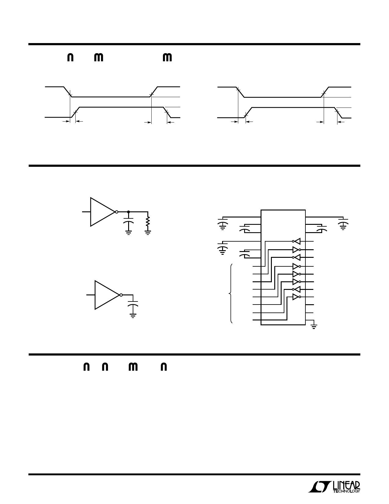
SWITCHI G TI E WAVEFOR S
DRIVER
INPUT
1.4V
DRIVER
OUTPUT
0V
t LHD
1.4V
t HLD
VCC
0V
V+
0V
V–
LTC1348 • F01
Figure 1. Driver Propagation Delay Timing
RX
1.7V
INPUT
RX
OUTPUT
0.8V
t LHR
VCC
1.3V
0V
t HLR
2.4V VCC
0V
LTC1348 • F02
Figure 2. Receiver Propagation Delay Timing
TEST CIRCUITS
DRIVER
INPUT
DRIVER
DRIVER
OUTPUT
51pF 3k
LTC1348 • F03
Figure 3. Driver Timing Test Load
RX INPUT
RX
RX
OUTPUT
51pF
LTC1348 • F04
Figure 4. Receiver Timing Test Load
ESD Test Circuit
0.1µF
V+
1
C2+ 2
0.1µF
0.1µF
VCC
3
C2– 4
C1+ 5
0.1µF
6
C1– 7
DR1 OUT
8
RX1 IN
9
DR2 OUT
RS232 LINE PINS
PROTECTED TO ±10kV
10
RX2 IN
11
RX3 IN
12
RX4 IN
13
DR3 OUT
14
RX5 IN
LTC1348
28
V–
27 C3+
26
0.1µF
25 C3–
DR1 IN
24 RX1 OUT
23
DR2 IN
22
RX2 OUT
21
RX3 OUT
20
RX4 OUT
19 DR3 IN
18
RX5 OUT
17
DREN
16 RXEN
15
GND
LT1348 • TC
0.1µF
APPLICATIONS INFORMATION
Power Supply
The LTC1348 includes an onboard voltage-tripling charge
pump capable of generating ±8V from a single 3.3V
supply. This allows the LTC1348 drivers to provide guar-
anteed ±5V RS232-compliant voltage levels with a 3.3V
supply. With all outputs loaded with 3kΩ, the LTC1348
can typically swing ±5V with voltages as low as 2.85V. It
will meet the ±3.7V EIA562 levels with supply voltages as
low as 2.2V. The charge pump requires three external
flying capacitors to operate; 0.1µF ceramic capacitors are
adequate for most applications. For applications requiring
extremely high data rates or abnormally heavy output
loads, 0.33µF flying capacitors are recommended. Bypass
and output capacitor values should match those of the
flying capacitors and all capacitors should be mounted as
close to the package as possible.
6
Share Link: 