TGF4230-EEU Просмотр технического описания (PDF) - TriQuint Semiconductor
Номер в каталоге
Компоненты Описание
производитель
TGF4230-EEU Datasheet PDF : 7 Pages
| |||
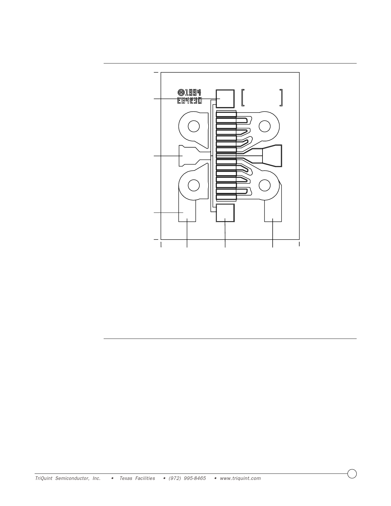
MECHANICAL DRAWING
0.699
0.601
TGF4230-EEU
2
R/C**
0.350
1
4
NOTES
0.099
3
0.0
0.0
0.097
0.264
0.471
0.572
Units: Millimeters
Thickness: 0.102
Chip size ± 0.0508
Bond pad 1 (gate): 0.072 x 0.075
Bond pad 2 (gate): 0.075 x 0.075*
Bond pad 3 (gate): 0.075 x 0.075*
Bond pad 4 (drain): 0.083 x 0.077
Minimum connections to Bond Pads 1 and 4. Sources are connected to backside metalization.
* Alternate gate pads used for paralleling TGF4230s or for multiple gate wir es.
** Wafer unique Row/Column data is recorded in brackets.
Gate bias supplies should be designed to sink or source gate current. The magnitude and direction of the gate
current is a function of bias point, load impedance, and drive level.
7
TriQuint Semiconductor, Inc. • Texas Facilities • (972) 995-8465 • www.triquint.com
Share Link: 