RFL1N08 Просмотр технического описания (PDF) - Intersil
Номер в каталоге
Компоненты Описание
производитель
RFL1N08 Datasheet PDF : 4 Pages
| |||
RFL1N08, RFL1N10
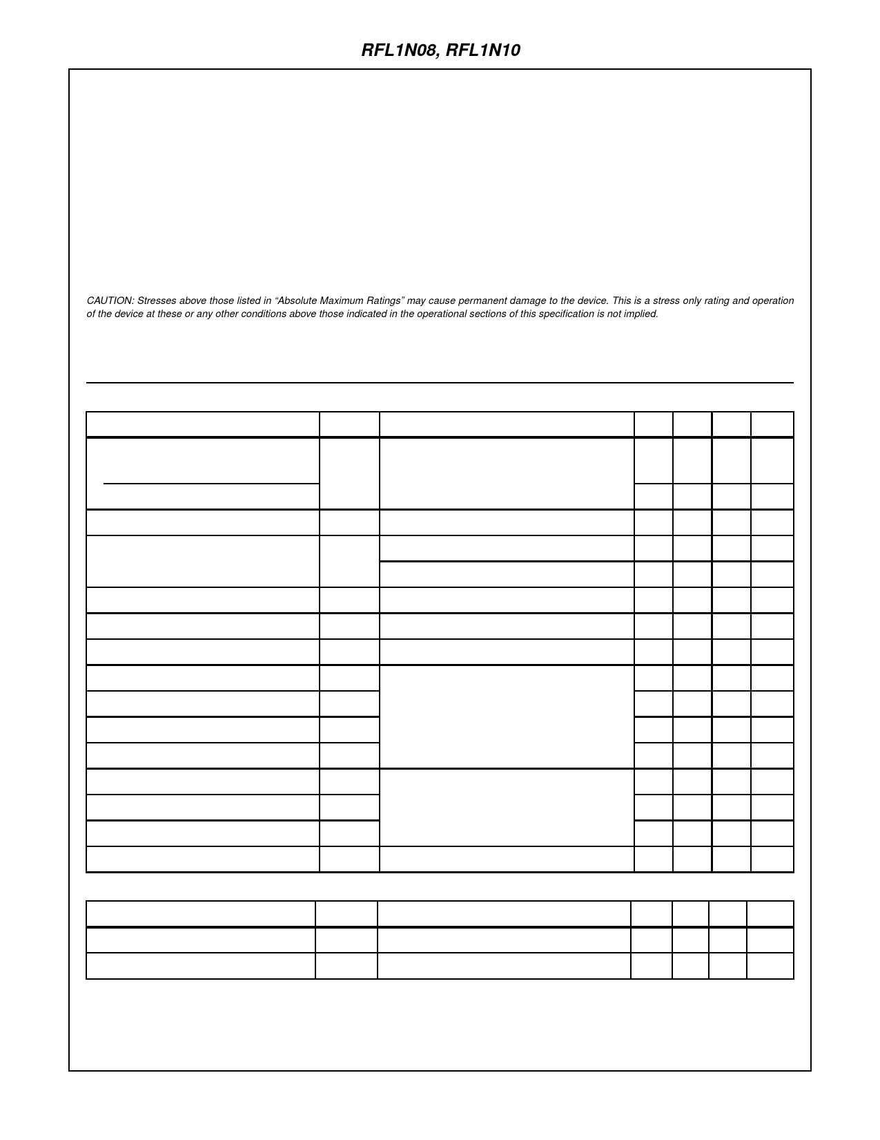
Absolute Maximum Ratings TC = 25oC, Unless Otherwise Specified
RFL1N08
RFL1N10
UNITS
Drain to Source Voltage (Note 1) . . . . . . . . . . . . . . . . . . . . . . . . . . . . . . . VDS
Drain to Gate Voltage (RGS = 20kΩ) (Note 1) . . . . . . . . . . . . . . . . . . . . VDGR
Continuous Drain Current. . . . . . . . . . . . . . . . . . . . . . . . . . . . . . . . . . . . . . . ID
Pulsed Drain Current (Note 3 . . . . . . . . . . . . . . . . . . . . . . . . . . . . . . . . . . .IDM
Gate to Source Voltage . . . . . . . . . . . . . . . . . . . . . . . . . . . . . . . . . . . . . . VGS
Maximum Power Dissipation . . . . . . . . . . . . . . . . . . . . . . . . . . . . . . . . . . . PD
Linear Derating Factor . . . . . . . . . . . . . . . . . . . . . . . . . . . . . . . . . . . . . . . . . . .
Operating and Storage Temperature . . . . . . . . . . . . . . . . . . . . . . . . TJ, TSTG
Maximum Temperature for Soldering
Leads at 0.063in (1.6mm) from Case for 10s . . . . . . . . . . . . . . . . . . . . . .TL
80
80
1
5
±20
8.33
0.0667
-55 to 150
260
100
100
1
5
±20
8.33
0.0667
-55 to 150
260
V
V
A
A
V
W
W/oC
oC
oC
CAUTION: Stresses above those listed in “Absolute Maximum Ratings” may cause permanent damage to the device. This is a stress only rating and operation
of the device at these or any other conditions above those indicated in the operational sections of this specification is not implied.
NOTE:
1. TJ = 25oC to 125oC.
Electrical Specifications TC = 25oC, Unless Otherwise Specified
PARAMETER
SYMBOL
TEST CONDITIONS
MIN TYP MAX UNITS
Drain to Source Breakdown Voltage
RFL1N08
BVDSS ID = 250µA, VGS = 0V
80
-
-
V
RFL1N10
100 -
-
V
Gate Threshold Voltage
VGS(TH) VDS = VGS, ID = 250µA, (Figure 8)
2
Zero Gate Voltage Drain Current
IDSS VGS = Rated BVDSS, VGS = 0V
-
VDS = 0.8 x Rated BVDSS, VGS = 0V, TJ = 125oC -
On-State Drain Current (Note 2)
ID(ON) VDS > ID(ON) x rDS(ON)MAX, VGS = 10V
1
Gate to Source Leakage Current
IGSS VGS = ±20V
-
Drain to Source On Resistance
rDS(ON) ID = 5.6A, VGS = 10V, (Figures 6, 7)
Turn-On Delay Time
Rise Time
Turn-Off Delay Time
td(ON) VDD = 50V, VGS = 10V, ID ≈ 1A, RG = 50Ω,
-
RL = 50Ω (Figures 10, 11, 12)
tr
MOSFET Switching Times are Essentially Inde- -
pendent of Operating Temperature
td(OFF)
-
Fall Time
tf
-
Input Capacitance
Output Capacitance
CISS VDS = 25V, VGS = 0V, f = 1MHz
-
(Figure 9)
COSS
-
Reverse Transfer Capacitance
CRSS
-
Thermal Resistance Junction to Case
RθJC
-
Source to Drain Diode Specifications
-
4
V
-
1
µA
-
25 µA
-
-
A
- ±100 nA
1.200 Ω
17 25 ns
30 45 ns
30 45 ns
30 50 ns
- 200 pF
-
80
pF
-
25
pF
-
oC/W
PARAMETER
SYMBOL
TEST CONDITIONS
Source to Drain Diode Voltage (Note 2)
Reverse Recovery Time
VSD
TJ = 25oC, ISD = 1A, VGS = 0V
trr
TJ = 25oC, ISD = 1A, dISD/dt = 100A/µs
NOTES:
2. Pulse test: pulse width ≤ 300µs, duty cycle ≤ 2%.
3. Repetitive rating: pulse width limited by maximum junction temperature.
MIN TYP MAX UNITS
-
- 1.4
V
- 100 -
ns
5-2
Share Link: 