BGA2771 Просмотр технического описания (PDF) - NXP Semiconductors.
Номер в каталоге
Компоненты Описание
производитель
BGA2771 Datasheet PDF : 11 Pages
| |||
NXP Semiconductors
MMIC wideband amplifier
Product specification
BGA2771
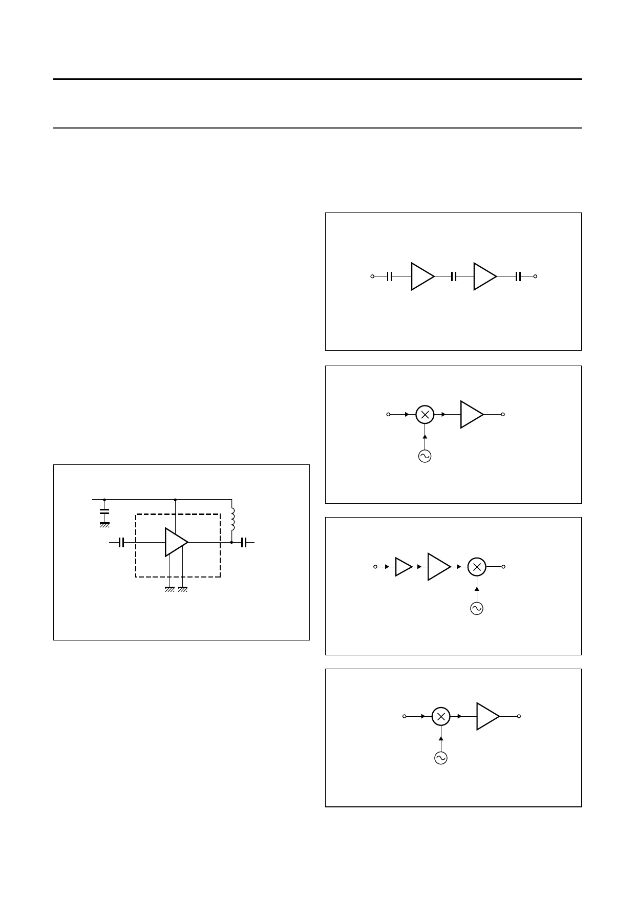
APPLICATION INFORMATION
Figure 2 shows a typical application circuit for the
BGA2771 MMIC. The device is internally matched to 50 ,
and therefore does not need any external matching. The
value of the input and output DC blocking capacitors C2
and C3 should be not more than 100 pF for applications
above 100 MHz. However, when the device is operated
below 100 MHz, the capacitor value should be increased.
The nominal value of the RF choke L1 is 100 nH. At
frequencies below 100 MHz this value should be
increased to 220 nH. At frequencies above 1 GHz a much
lower value must be used (e.g. 10 nH) to improve return
losses. For optimal results, a good quality chip inductor
such as the TDK MLG 1608 (0603), or a wire-wound SMD
type should be chosen.
Both the RF choke L1 and the 22 nF supply decoupling
capacitor C1 should be located as closely as possible to
the MMIC.
Separate paths must be used for the ground planes of the
ground pins GND1 and GND2, and these paths must be as
short as possible. When using vias, use multiple vias per
pin in order to limit ground path inductance.
In Fig.6 the MMIC is used as a driver to the power amplifier
as part of a transmitter circuit. Good linear performance
and matched input and output offer quick design solutions
in such applications.
handbook, halfpaDgCe -block
100 pF
input
DC-block
100 pF
DC-block
100 pF
output
MGU437
Fig.3 Simple cascade circuit.
handbook, halfpage
from RF
circuit
mixer
oscillator
wideband
amplifier
to IF circuit
or demodulator
MGU438
handbookV, shalfpage
C1
RF input
C2
RF in
Vs
RF out
GND1 GND2
L1
RF output
C3
MGU436
Fig.2 Typical application circuit.
Fig.4 IF amplifier application.
handbook, halfpage
antenna
LNA
mixer
wideband
amplifier
oscillator
to IF circuit
or demodulator
MGU439
Fig.5 RF amplifier application.
Figure 3 shows two cascaded MMICs. This configuration
doubles overall gain while preserving broadband
characteristics. Supply decoupling and grounding
conditions for each MMIC are the same as those for the
circuit of Fig.2.
The excellent wideband characteristics of the MMIC make
it and ideal building block in IF amplifier applications such
as LBNs (see Fig.4).
As a buffer amplifier between an LNA and a mixer in a
receiver circuit, the MMIC offers an easy matching, low
noise solution (see Fig.5).
handbforookm, hmalfopdaguelation
or IF circuit
mixer
oscillator
wideband
amplifier
to power
amplifier
MGU440
Fig.6 Power amplifier driver application.
2002 Aug 06
4
Share Link: 