BF1208 Просмотр технического описания (PDF) - NXP Semiconductors.
Номер в каталоге
Компоненты Описание
производитель
BF1208 Datasheet PDF : 23 Pages
| |||
NXP Semiconductors
BF1208
Dual N-channel dual gate MOSFET
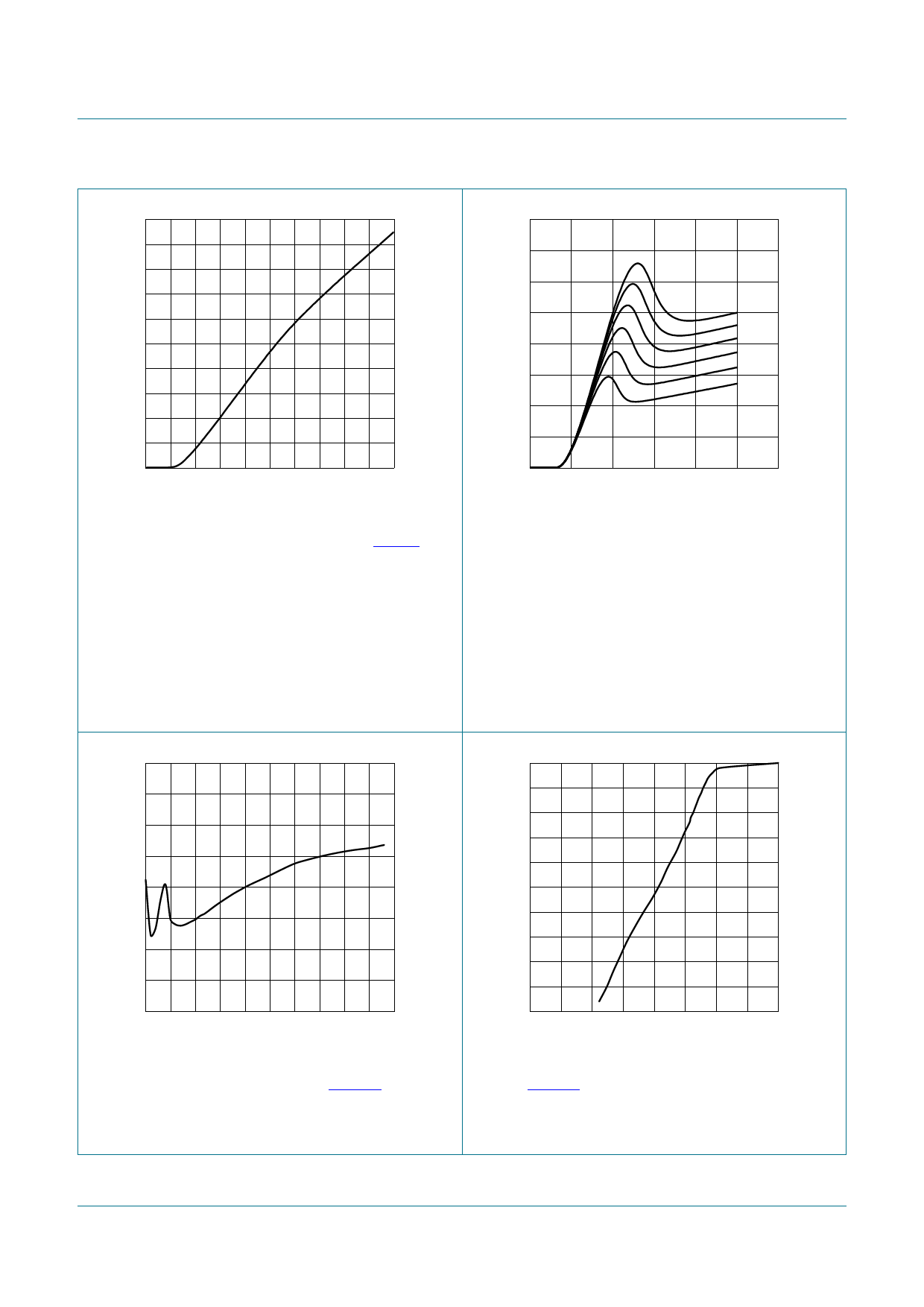
20
ID
(mA)
16
12
8
4
001aaa558
32
ID
(mA)
24
16
8
001aaa559
(1)
(2)
(3)
(4)
(5)
(6)
0
0
1
2
3
4
5
Vsup (V)
VDS(A) = VDS(B) = Vsupply; VG2-S = 4 V; Tj = 25 C;
RG1 = 150 k (connected to ground); see Figure 3.
Fig 8.
Amplifier A: drain current of amplifier A as a
function of supply voltage of A and B
amplifier; typical values
120
Vunw
(dBμV)
110
001aac195
100
90
0
0
2
4
6
VG2-S (V)
(1) VDS(B) = 5 V.
(2) VDS(B) = 4.5 V.
(3) VDS(B) = 4 V.
(4) VDS(B) = 3.5 V.
(5) VDS(B) = 3 V.
(6) VDS(B) = 2.5 V.
VDS(A) = 5 V; VG1-S(B) = 0 V; gate1 (A) = open;
Tj = 25 C.
Fig 9. Amplifier A: drain current as a function of
gate2 voltage; typical values
0
gain
reduction
(dB)
10
20
30
40
001aac196
80
0
10
20
30
40
50
gain reduction (dB)
VDS(A) = VDS(B) = 5 V; VG1-S(B) = 0 V; fw = 50 MHz;
funw = 60 MHz; Tamb = 25 C; see Figure 33.
Fig 10. Amplifier A: unwanted voltage for 1 %
cross-modulation as a function of gain
reduction; typical values
50
0
1
2
3
4
VAGC (V)
VDS(A) = VDS(B) = 5 V; VG1-S(B) = 0 V; f = 50 MHz; see
Figure 33.
Fig 11. Amplifier A: gain reduction as a function of
AGC voltage; typical values
BF1208
Product data sheet
All information provided in this document is subject to legal disclaimers.
Rev. 2 — 7 September 2011
© NXP B.V. 2011. All rights reserved.
8 of 23
Share Link: 