BD238 Просмотр технического описания (PDF) - ON Semiconductor
Номер в каталоге
Компоненты Описание
производитель
BD238 Datasheet PDF : 4 Pages
| |||
BD237 (NPN), BD234 (PNP), BD238 (PNP)
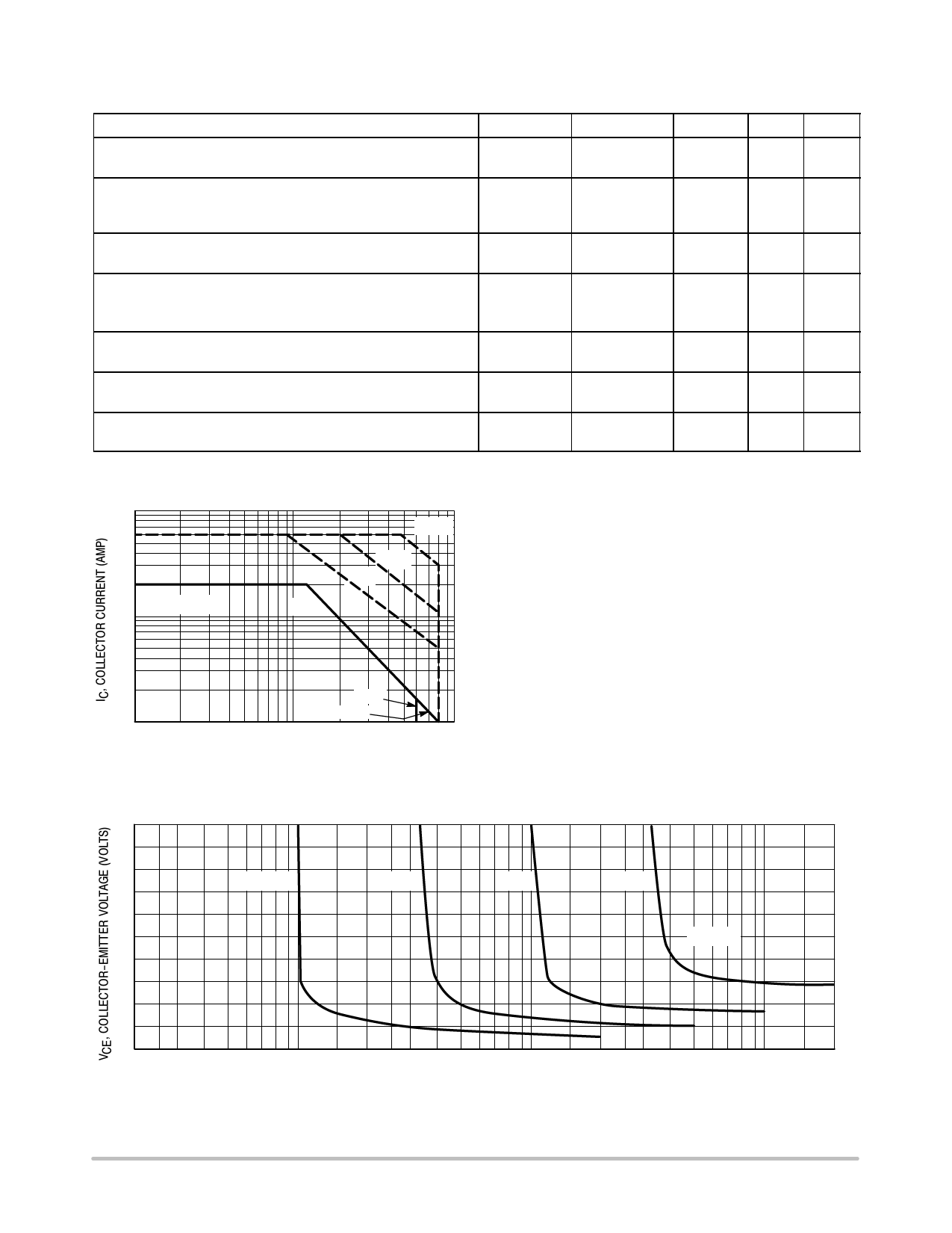
ÎÎÎÎÎÎÎÎÎÎÎÎÎÎÎÎÎÎÎÎÎÎÎÎÎÎÎÎÎÎÎÎÎ ELECTRICAL CHARACTERISTICS (TC = 25_C unless otherwise noted)
ÎÎÎÎÎÎÎÎÎÎÎÎÎÎÎÎÎÎÎÎÎÎÎÎÎÎÎÎÎÎÎÎÎ Characteristic
Symbol
Type
Min
ÎÎÎÎÎÎÎÎÎÎÎÎÎÎÎÎÎÎÎÎÎÎÎÎÎÎÎÎÎÎÎÎÎ Collector−Emitter Sustaining Voltage (Note 1)
ÎÎÎÎÎÎÎÎÎÎÎÎÎÎÎÎÎÎÎÎÎÎÎÎÎÎÎÎÎÎÎÎÎ (IC = 0.1 Adc, IB = 0)
ÎÎÎÎÎÎÎÎÎÎÎÎÎÎÎÎÎÎÎÎÎÎÎÎÎÎÎÎÎÎÎÎÎ Collector Cutoff Current
(VCB = 100 Vdc, IE = 0)
ÎÎÎÎÎÎÎÎÎÎÎÎÎÎÎÎÎÎÎÎÎÎÎÎÎÎÎÎÎÎÎÎÎ (VCB = 60 Vdc, IE = 0)
ÎÎÎÎÎÎÎÎÎÎÎÎÎÎÎÎÎÎÎÎÎÎÎÎÎÎÎÎÎÎÎÎÎ Emitter Cutoff Current
ÎÎÎÎÎÎÎÎÎÎÎÎÎÎÎÎÎÎÎÎÎÎÎÎÎÎÎÎÎÎÎÎÎ (VBE = 5.0 Vdc, IC = 0)
ÎÎÎÎÎÎÎÎÎÎÎÎÎÎÎÎÎÎÎÎÎÎÎÎÎÎÎÎÎÎÎÎÎ DC Current Gain
(IC = 0.15 A, VCE = 2.0 V)
ÎÎÎÎÎÎÎÎÎÎÎÎÎÎÎÎÎÎÎÎÎÎÎÎÎÎÎÎÎÎÎÎÎ (IC = 1.0 A, VCE = 2.0 V)
ÎÎÎÎÎÎÎÎÎÎÎÎÎÎÎÎÎÎÎÎÎÎÎÎÎÎÎÎÎÎÎÎÎ Collector−Emitter Saturation Voltage (Note 1)
ÎÎÎÎÎÎÎÎÎÎÎÎÎÎÎÎÎÎÎÎÎÎÎÎÎÎÎÎÎÎÎÎÎ (IC = 1.0 Adc, IB = 0.1 Adc)
ÎÎÎÎÎÎÎÎÎÎÎÎÎÎÎÎÎÎÎÎÎÎÎÎÎÎÎÎÎÎÎÎÎ Base−Emitter On Voltage (Note 1)
ÎÎÎÎÎÎÎÎÎÎÎÎÎÎÎÎÎÎÎÎÎÎÎÎÎÎÎÎÎÎÎÎÎ (IC = 1.0 Adc, VCE = 2.0 Vdc)
V(BR)CEO
BD237, BD238
80
BD234
45
ICBO
BD237, BD238
−
BD234
−
IEBO
−
−
hFE1
hFE2
−
40
−
25
VCE(sat)
−
−
VBE(on)
−
−
Current−Gain − Bandwidth Product
ÎÎÎÎÎÎÎÎÎÎÎÎÎÎÎÎÎÎÎÎÎÎÎÎÎÎÎÎÎÎÎÎÎÎÎÎÎÎÎÎÎÎÎÎÎÎÎÎÎÎÎÎÎÎÎÎÎÎÎÎÎÎÎÎÎÎ (IC = 250 mAdc, VCE = 10 Vdc, f = 1.0 MHz)
fT
−
3.0
Max Unit
−
Vdc
−
mAdc
0.1
0.1
1.0 mAdc
−
−
−
0.6
Vdc
1.3
Vdc
−
MHz
1. Pulse Test: Pulse Width x 300 ms, Duty Cycle x 2.0%.
10
3
TJ = 150°C
1
100 ms
1 ms
5 ms
dc
0.3
0.1
1
3
BD236
BD237
10
30
100
VCE, COLLECTOR−EMITTER VOLTAGE (VOLTS)
Figure 1. Active Region Safe Operating Area
The Safe Operating Area Curves indicate IC−VCE limits
below which the device will not enter secondary breakdown.
Collector load lines for specific circuits must fall within the
applicable Safe Area to avoid causing a catastrophic failure.
To insure operation below the maximum TJ,
power−temperature derating must be observed for both
steady state and pulse power conditions.
1.0
0.8
IC = 0.1 A
0.25 A
0.5 A
1.0 A
0.6
TJ = 25°C
0.4
0.2
0
0.2 0.3
0.5
1.0
2.0 3.0
5.0
10
20 30
50
IB, BASE CURRENT (mA)
Figure 2. Collector Saturation Region
100
200
http://onsemi.com
2
Share Link: 