HSP48901JC-30 Просмотр технического описания (PDF) - Intersil
Номер в каталоге
Компоненты Описание
производитель
HSP48901JC-30 Datasheet PDF : 9 Pages
| |||
HSP48901
Initialization Register
The Initialization Register is used to appropriately configure
the convolver for a particular application. It is loaded through
the use of the CIN0-7 bus along with the LD input. Bit-0
defines the input data and coefficients format (unsigned or
two's complement); Bit-1 defines the mode of operation (1-D
or 2-D); and Bit-2 and Bit-3 determine the type of rounding to
occur on the DOUT0-19 bus; The complete definition of the
Initialization Register bits is given in Table 1.
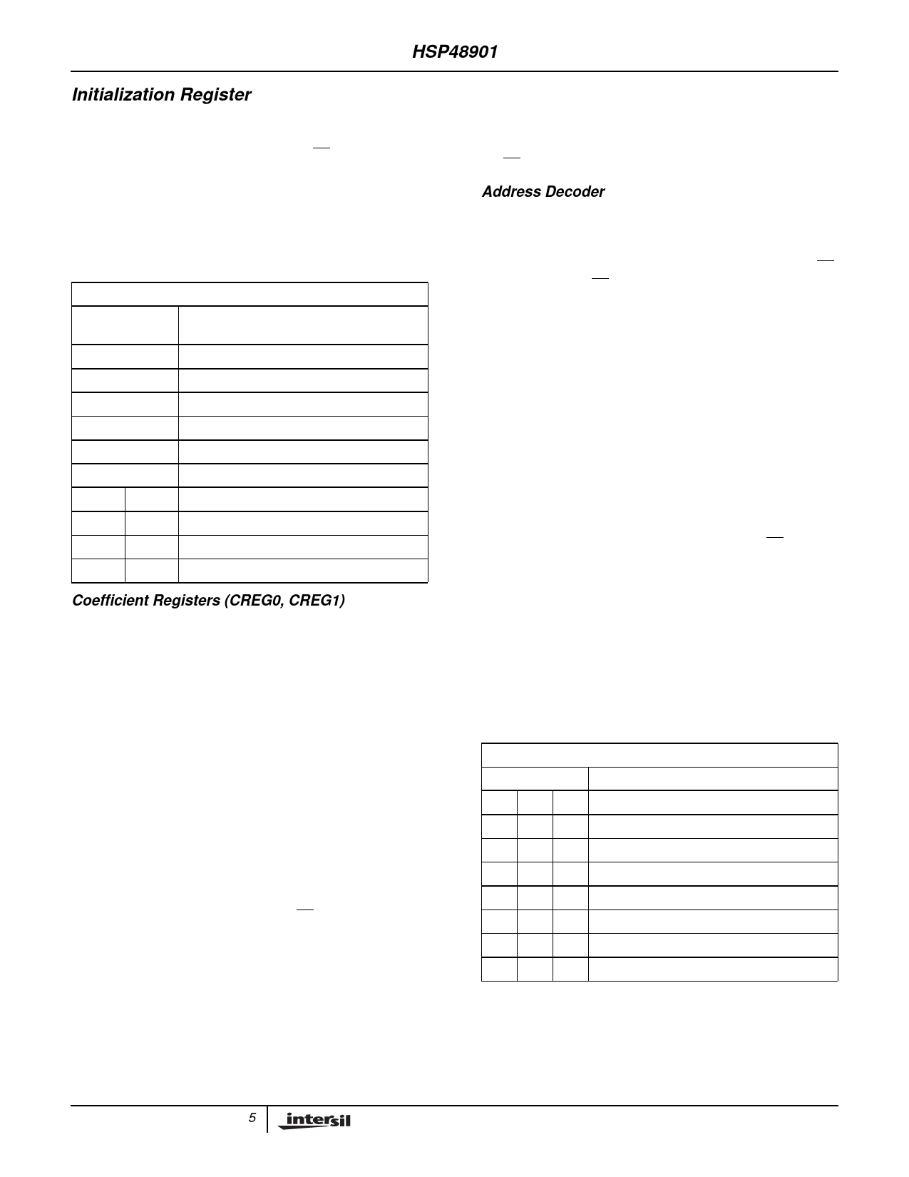
TABLE 1. INITIALIZATION REGISTER
INITIALIZATION REGISTER
BIT 0
FUNCTION = INPUT AND COEFFICIENT
DATA FORMAT
0
Unsigned Integer Format
1
Two’s Complement Format
BIT 1
FUNCTION = OPERATING MODE
0
1-D 9-Tap Filter
1
2-D 3 x 3 Filter
3 BIT 2
FUNCTION = OUTPUT ROUNDING
0
0 No Rounding
0
1 Round to 16 Bits (i.e., DOUT19-4)
1
0 Round to 8 Bits (i.e., DOUT19-12)
1
1 Not Valid
Coefficient Registers (CREG0, CREG1)
The control logic contains two coefficient register banks,
CREG0 and CREG1. Each of these register banks is
capable of storing nine 8-bit filter coefficient values (3 x 3
Kernel). The output of the registers are connected to the
coefficient input of the corresponding multiplier in the 3 x 3
multiplier array (designated A through I). The register bank
to be used for the convolution is selectable by writing to the
appropriate address (see address decoder). All registers in a
given bank are enabled simultaneously, and one of the
banks is always active.
For most applications, only one of the register banks is
necessary. The user can simply load CREG0 after power up,
and use it for the entire convolution operation. (CREG0 is the
Default Register). The alternate register bank allows the
user to maintain two sets of filter coefficients and switch
between them in real time. The coefficient masks are loaded
via the CIN0-7 bus by using A0-2 and LD. The selection of
the particular register bank to be used in processing is also
done by writing to the appropriate address (See address
decoder). For example, if CREG0 is being used to provide
coefficients to the multipliers, CREG1 can be updated at a
low rate by an external processor; then, at the proper time,
CREG1 can be selected, so that the new coefficient mask is
used to process the data. Thus, no clock cycles have been
lost when changing between alternate 3 x 3 filter kernels.
The nine coefficients must be loaded sequentially over the
CIN0-7 bus from A to I. The address of CREG0 or CREG1 is
placed on A0-2, and then the coefficients are written to the
corresponding Coefficient Register one at a time by using
the LD input.
Address Decoder
The address decoder (see Figure 1) is used for writing to the
control logic of the HSP48901. Loading an Internal Register
is done by selecting the Destination Register with the A0-2
address lines, placing the data on CIN0-7, and asserting LD
control line. When LD goes high, the data on ClN0-7 is
latched into the addressed register. The address map for the
A0-2 bus is shown in Table 2.
While loading of the control logic registers is asynchronous
to CLK, the target register in the control logic is being read
synchronous to the internal clock. Therefore, care must be
taken when modifying the convolver setup parameters
during processing to avoid changing the contents of the
registers near a rising edge of CLK. The required setup time
relative to CLK is given by the specification TLCS. For
example, in order to change the active coefficient register
from CREG0 to CREG1 during an active convolution
operation, a write will be performed to the address for
selecting CREG1 for internal processing (A0-2 = 110). In
order to provide proper uninterrupted operation, LD should
be deasserted at least TLCS prior to the next rising edge of
CLK. Failure to meet this setup time may result in
unpredictable results on the output of the convolver. Keep in
mind that this requirement applies only to the case where
changes are being made in the control logic during an active
convolution operation. In a typical convolver configuration
routine, where the configuration data is loaded prior to the
actual convolution operation, this specification would not
apply.
TABLE 2. ADDRESS MAPS
CONTROL LOGIC ADDRESS MAP
A2-0
FUNCTION
0 0 0 Reserved for Future Use.
0 0 1 Reserved for Future Use.
0 1 0 Load Coefficient Register 0 (CREG0).
0 1 1 Load Coefficient Register 1 (CREG1).
1 0 0 Load Initialization Register (INT).
1 0 1 Select CREG0 for Internal Processing.
1 1 0 Select CREG1 for Internal Processing.
1 1 1 No Operation.
5
Share Link: 