ATTL7582BC Просмотр технического описания (PDF) - Agere -> LSI Corporation
Номер в каталоге
Компоненты Описание
производитель
ATTL7582BC Datasheet PDF : 16 Pages
| |||
Data Sheet
November 1999
L7582 Tip Ring Access Switch
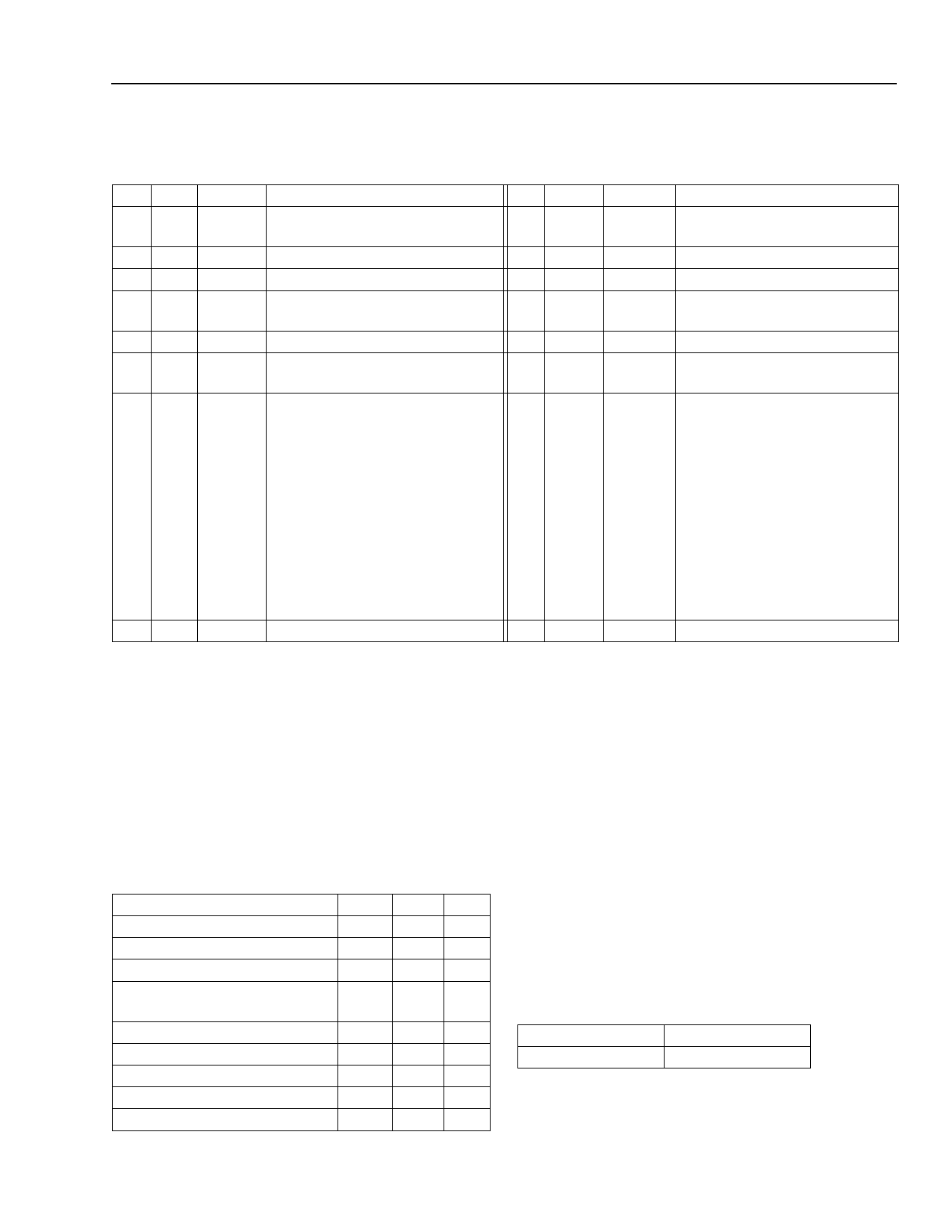
Pin Information (continued)
Table 1. Pin Descriptions
DIP SOG Symbol
Description
DIP
1 1 FGND Fault ground.
16
22
TBAT Connect to TIP on SLIC side.
15
3 3 TLINE Connect to TIP on line side.
14
4 4 TRINGING Connect to return ground for ring- 13
ing generator.
5 5 TACCESS Test access.
12
66
VDD 5 V supply.
11
77
TSD Temperature shutdown pin. Can 10
be used as a logic level input or
output. See Table 13, Truth Table,
and the Switching Behavior sec-
tion of this data sheet for input pin
description. As an output, will
read 5 V when device is in its
operational mode and 0 V in the
thermal shutdown mode. To dis-
able the thermal shutdown mech-
anism, tie this pin to 5 V (not
recommended).
8 8 DGND Digital ground.
9
SOG
16
15
14
13
12
11
10
9
Symbol
Description
VBAT Battery voltage. Used as a ref-
erence for protection circuit.
RBAT Connect to RING on SLIC side.
RLINE Connect to RING on line side.
RRINGING Connect to ringing generator.
RACCESS Test access.
LATCH Data latch control, active-high,
transparent low.
INRING Logic level input switch control.
INACCESS Logic level input switch control.
Absolute Maximum Ratings
Handling Precautions
Stresses in excess of the absolute maximum ratings
can cause permanent damage to the device. These are
absolute stress ratings only. Functional operation of the
device is not implied at these or any other conditions in
excess of those given in the operational sections of the
data sheet. Exposure to absolute maximum ratings for
extended periods can adversely affect device reliability.
Table 2. Absolute Maximum Ratings Parameters
Parameter
Min Max Unit
Operating Temperature Range –40 110 °C
Storage Temperature Range –40 150 °C
Relative Humidity Range
5
95 %
Pin Soldering Temperature (t = — 260 °C
10 s max)
5 V Power Supply
—
7
V
Battery Supply
— –85 V
Logic Input Voltage
—
7
V
Input-to-output Isolation
— 330 V
Pole-to-pole Isolation
— 330 V
Although protection circuitry has been designed into
this device, proper precautions should be taken to
avoid exposure to electrostatic discharge (ESD) during
handling and mounting. Lucent Technologies Micro-
electronics Group employs a human-body model
(HBM) and a charged-device model (CDM) for ESD-
susceptibility testing and protection design evaluation.
ESD voltage thresholds are dependent on the circuit
parameters used to define the model. No industry-wide
standard has been adopted for CDM. However, a stan-
dard HBM (resistance = 1500 Ω, capacitance = 100 pF)
is widely used and therefore can be used for compari-
son purposes. The HBM ESD threshold presented
here was obtained by using these circuit parameters.
Table 3. HBM ESD Threshold Voltage
Device
L7582
Rating
1000 V
Lucent Technologies Inc.
3
Share Link: 