ATF1502AS-7AC44 Просмотр технического описания (PDF) - Atmel Corporation
Номер в каталоге
Компоненты Описание
производитель
ATF1502AS-7AC44 Datasheet PDF : 18 Pages
| |||
macrocell. (This feature is automatically implemented by
the fitter software). In addition to D, T, JK and SR opera-
tion, the flip flop can also be configured as a flow-through
latch. In this mode, data passes through when the clock is
high and is latched when the clock is low.
The clock itself can either be one of the Global CLK Signal
GCK[0 : 2] or an individual product term. The flip flop
changes state on the clock’s rising edge. When the GCK
signal is used as the clock, one of the macrocell product
terms can be selected as a clock enable. When the clock
enable function is active and the enable signal (product
term) is low, all clock edges are ignored. The flip flop’s
asynchronous reset signal (AR) can be either the Global
Clear (GCLEAR), a product term, or always off. AR can
also be a logic OR of GCLEAR with a product term. The
asynchronous preset (AP) can be a product term or always
off.
Output Select and Enable
The ATF1502AS macrocell output can be selected as reg-
istered or combinatorial. The buried feedback signal can be
either combinatorial or registered signal regardless of
whether the output is combinatorial or registered.
The output enable multiplexer (MOE) controls the output
enable signals. Any buffer can be permanently enabled for
simple output operation. Buffers can also be permanently
disabled to allow use of the pin as an input. In this configu-
ration all the macrocell resources are still available, includ-
ing the buried feedback, expander and CASCADE logic.
The output enable for each macrocell can be selected as
either of the two dedicated OE input pins as an I/O pin con-
figured as an input, or as an individual product term.
Global Bus/Switch Matrix
The global bus contains all input and I/O pin signals as well
as the buried feedback signal from all 32 macrocells. The
Switch Matrix in each Logic Block receives as its inputs all
signals from the global bus. Under software control, up to
40 of these signals can be selected as inputs to the Logic
Block.
Foldback Bus
Each macrocell also generates a foldback product term.
This signal goes to the regional bus and is available to 4
macrocells. The foldback is an inverse polarity of one of the
macrocell’s product terms. The 4 foldback terms in each
region allows generation of high fan-in sum terms (up to 9
product terms) with a small additional delay.
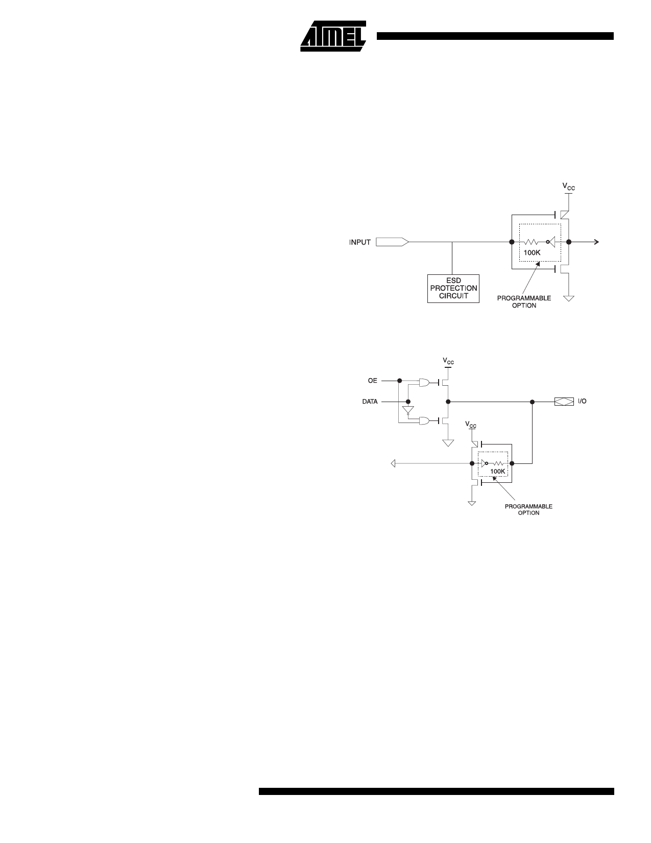
Programmable Pin-Keeper Option for
Inputs and I/Os
The ATF1502AS offers the option of programming all input
and I/O pins so that pin keeper circuits can be utilized.
When any pin is driven high or low and then subsequently
left floating, it will stay at that previous high or low level.
This circuitry prevents unused input and I/O lines from
floating to intermediate voltage levels, which cause unnec-
essary power consumption and system noise. The keeper
circuits eliminate the need for external pull-up resistors and
eliminate their DC power consumption.
Input Diagram
I/O Diagram
Speed/Power Management
The ATF1502AS has several built-in speed and power
management features. The ATF1502AS contains circuitry
that automatically puts the device into a low power stand-
by mode when no logic transitions are occurring. This not
only reduces power consumption during inactive periods,
but also provides a proportional power savings for most
applications running at system speeds below 50 MHz. This
feature may be selected as a design option.
To further reduce power, each ATF1502AS macrocell has
a Reduced Power bit feature. This feature allows individual
macrocells to be configured for maximum power savings.
This feature may be selected as a design option.
The ATF1502ASs also has an optional power down mode.
In this mode, current drops to below 10 mA. When the
power down option is selected, either PD1 or PD2 pins (or
both) can be used to power down the part. The power down
4
ATF1502AS
Share Link: 