AT49BV8192A-10CI Просмотр технического описания (PDF) - Atmel Corporation
Номер в каталоге
Компоненты Описание
производитель
AT49BV8192A-10CI Datasheet PDF : 16 Pages
| |||

Features
• Single-voltage Read/Write Operation: 2.7V to 3.6V (BV), 3.0V to 3.6V (LV)
• Fast Read Access Time – 90 ns
• Internal Erase/Program Control
• Sector Architecture
– One 8K Word (16K Bytes) Boot Block with Programming Lockout
– Two 4K Word (8K Bytes) Parameter Blocks
– One 496K Word (992K Bytes) Main Memory Array Block
• Fast Sector Erase Time – 10 seconds
• Byte-by-byte or Word-by-word Programming – 30 µs Typical
• Hardware Data Protection
• Data Polling for End of Program Detection
• Low Power Dissipation
– 25 mA Active Current
– 50 µA CMOS Standby Current
• Typical 10,000 Write Cycles
Description
The AT49BV008A(T) and AT49BV8192A(T) are 3-volt, 8-megabit Flash memories
organized as 1,048,576 words of 8 bits each or 512K words of 16 bits each. Manufac-
tured with Atmel’s advanced nonvolatile CMOS technology, the devices offer access
times to 90 ns with power dissipation of just 67 mW at 2.7V read. When deselected,
the CMOS standby current is less than 50 µA.
The device contains a user-enabled “boot block” protection feature. Two versions of
the feature are available: the AT49BV008A/8192A locates the boot block at lowest
order addresses (“bottom boot”); the AT49BV008AT/8192AT locates it at highest
order addresses (“top boot”).
To allow for simple in-system reprogrammability, the AT49BV008A(T)/8192A(T) does
not require high input voltages for programming. Reading data out of the device is
similar to reading from an EPROM; it has standard CE, OE and WE inputs to avoid
(continued)
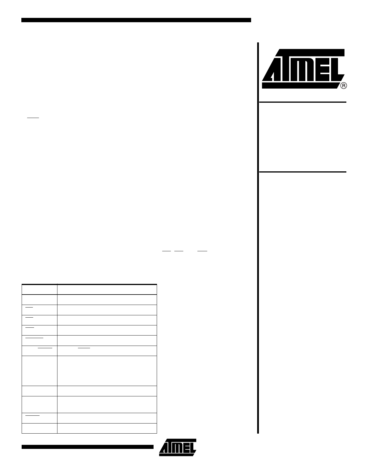
Pin Configurations
Pin Name
A0 - A18
CE
OE
WE
RESET
RDY/BUSY
VPP
I/O0 - I/O14
I/O15 (A-1)
BYTE
NC
Function
Addresses
Chip Enable
Output Enable
Write Enable
Reset
Ready/Busy Output
VPP can be left unconnected or
connected to VCC, GND, 5V or 12V.
The input has no effect on the
operation of the device.
Data Inputs/Outputs
I/O15 (Data Input/Output, Word Mode)
A-1 (LSB Address Input, Byte Mode)
Selects Byte or Word Mode
No Connect
8-megabit
(1M x 8/
512K x 16)
Flash Memory
AT49BV008A
AT49BV008AT
AT49BV8192A
AT49BV8192AT
AT49LV8192A
Rev. 1049I–03/01
1