AT25F512A Просмотр технического описания (PDF) - Atmel Corporation
Номер в каталоге
Компоненты Описание
производитель
AT25F512A Datasheet PDF : 19 Pages
| |||
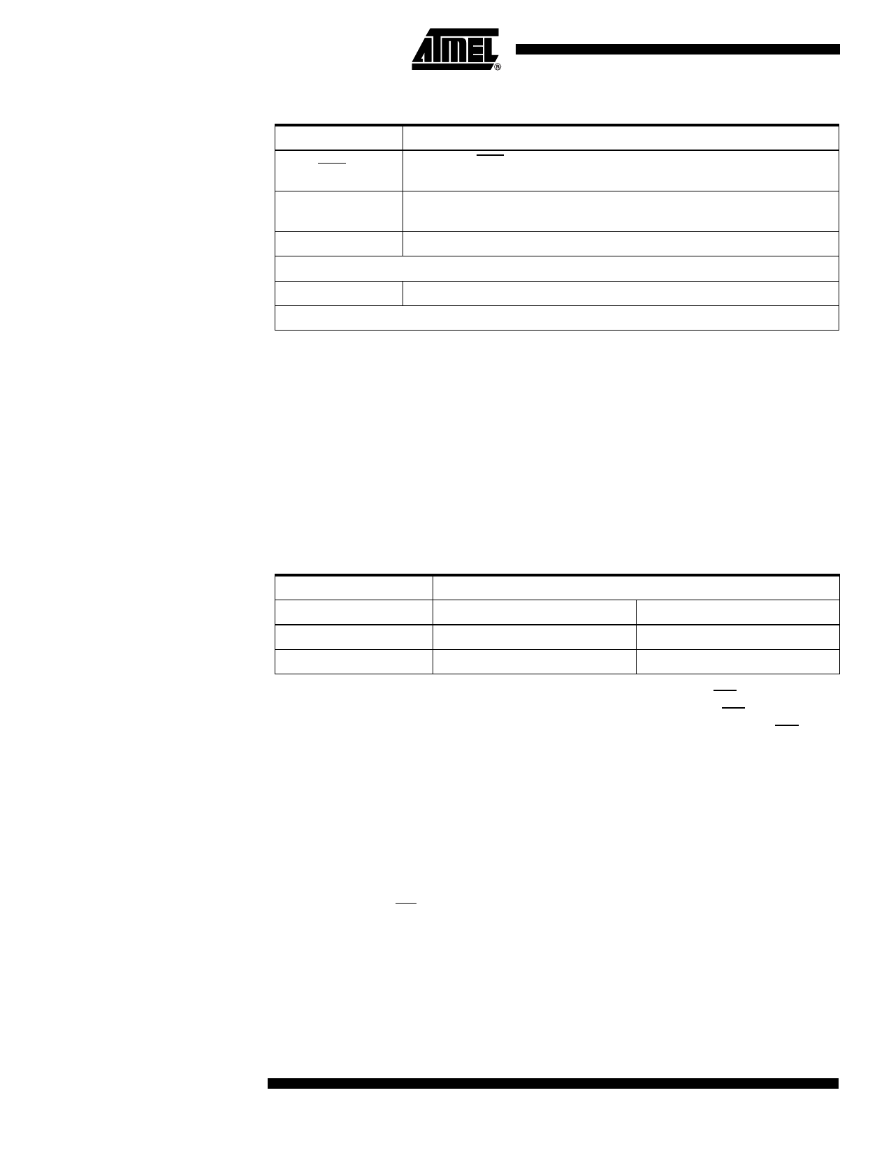
Table 7. Read Status Register Bit Definition
Bit
Definition
Bit 0 (RDY)
Bit 0 = “0” (RDY) indicates the device is ready. Bit 0 = “1” indicates the
write cycle is in progress.
Bit 1 (WEN)
Bit 1 = “0” indicates the device is not write enabled. Bit 1 = “1” indicates
the device is write enabled.
Bit 2 (BP0)
See Table 8.
Bits 3–6 are “0”s when device is not in an internal write cycle.
Bit 7 (WPEN)
See Table 9.
Bits 0–7 are “1”s during an internal write cycle.
READ PRODUCT ID (RDID): The RDID instruction allows the user to read the manufac-
turer and product ID of the device. The first byte after the instruction will be the
manufacturer code (1FH = ATMEL), followed by the device code, 65H.
WRITE STATUS REGISTER (WRSR): The WRSR instruction allows the user to select
two levels of protection for the AT25F512A. The AT25F512A is divided into two sectors
where all of the memory sectors can be protected (locked out) from write. Any of the
locked-out sectors will therefore be read only. The locked-out sectors and the corre-
sponding status register control bits are shown in Table 8.
The two bits, BP0 and WPEN, are nonvolatile cells that have the same properties and
functions as the regular memory cells (e.g., WREN, tWC, RDSR).
Table 8. Block Write Protect Bits
Status Register Bits
AT25F512A
BP0
Array Addresses Locked Out
Locked-out Sector(s)
0
None
None
1
000000–00FFFF
All sectors (1–2)
The WRSR instruction also allows the user to enable or disable the WP pin through the
use of the WPEN bit. Hardware write protection is enabled when the WP pin is low and
the WPEN bit is “1”. Hardware write protection is disabled when either the WP pin is
high or the WPEN bit is “0.” When the device is hardware write protected, writes to the
status register, including the block protect bit and the WPEN bit, and the locked-out sec-
tors in the memory array are disabled. The WRSR instruction is self-timed to
automatically erase and program BP0 and WPEN bits. In order to write the status regis-
ter, the device must first be write enabled via the WREN instruction. Then, the
instruction and data for the two bits are entered. During the internal write cycle, all
instructions will be ignored except RDSR instructions. The AT25F512A will automatically
return to write disable state at the completion of the WRSR cycle.
Note: When the WPEN bit is hardware write protected, it cannot be changed back to “0” as
long as the WP pin is held low.
8 AT25F512A
3345F–FLASH–11/06
Share Link: 